Camera Phone Technology 101
From sensors to optics to features, we'll run down the basics of mobile digital camera technology in this primer.
Get Tom's Hardware's best news and in-depth reviews, straight to your inbox.
You are now subscribed
Your newsletter sign-up was successful
Sensor
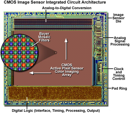
There are two main types of digital camera sensors: complementary metal-oxide semiconductor (CMOS) and charge-coupled device (CCD). Both technologies use a photoactive capacitor array to capture an image, where the charge accumulated in a given capacitor is proportional to the intensity of light at that location. In order to capture color information, the light must be filtered before it reaches the individual pixels. This is generally done with a Bayer color filter mosaic placed over the sensor’s pixel array.
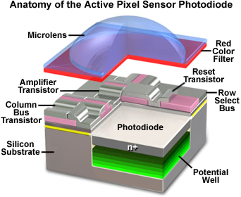
Where CMOS and CCD sensors differ, is in how the charge levels for each pixel are read from the array. A CCD sensor operates like a shift register, using an external control circuit to sequentially shift the charge from one capacitor to its neighbor. The charge from the last capacitor in the array is fed into an amplifier and the resulting voltages are processed and digitized. A CMOS sensor, however, performs these steps on-chip by including the necessary circuitry—usually consisting of at least three transistors and possibly other circuit elements—to process the voltage for each individual pixel and reset the photodiode.
Because CMOS technology allows for all of the circuitry (including advanced electronics such as noise reduction circuitry) to be built into each pixel, it uses less power, allows for smaller packages, and is capable of faster readouts, enabling features like 60fps and slow-motion video. The disadvantage of CMOS over CCD is that the circuitry takes up valuable real estate on the surface of the sensor. This means that for a given sensor size, a CCD will capture more light and offer better low-light performance than a CMOS sensor. CCD sensors also have higher dynamic range (there’s less noise because the circuitry is located off-chip) and better image uniformity (less chance for variation among amplifiers). The lower power consumption and smaller package sizes of CMOS sensors make them the ideal choice for smartphones and tablets. Larger format and professional cameras tend to use CCD sensors for their superior image quality.
Article continues belowAs can be seen in the image above, the photoactive area of this CMOS chip is only around 30%, with the majority dedicated to the transistors. In a CCD, the photoactive area would be more than twice as high, resulting in twice the light captured. However, with the ability to add noise reduction circuitry, the CMOS signal-to-noise ratio is good enough for most uses.
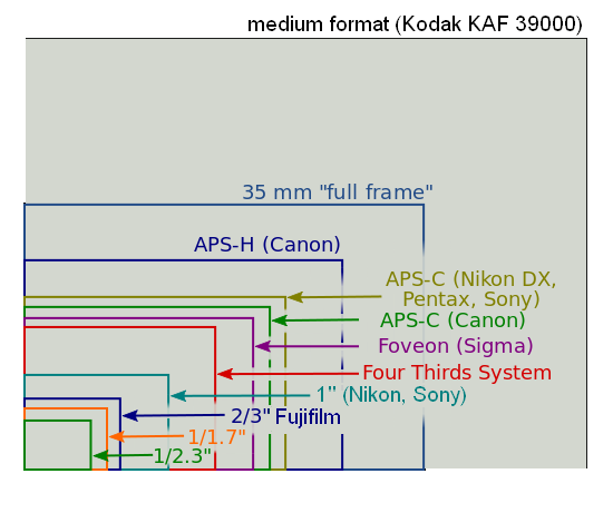
This image also shows why sensor size (also referred to as sensor format) is so important. Because the size of the transistors are fixed for a given process node, a larger sensor can either have a higher resolution (more pixels) or a higher percentage of photoactive area (larger pixels or pixel pitch).
A full-frame 35 mm sensor, used in many professional cameras, is defined as 36x24 mm. The APS-C sensor is approximately 22x15 mm, with slight variation by manufacturer, and is found in most high-end DSLRs and mirrorless cameras. The cameras found in mobile devices and point-and-shoots have sensor sizes that are a fraction of the APS-C sensor due to space and cost constraints. For example, the sensors in both the iPhone 6 and Samsung Galaxy S6 are smaller than the green 1/2.3” rectangle shown in the chart below.
[CREDIT: MarcusGR (Licensed under CC BY-SA 4.0)]
Get Tom's Hardware's best news and in-depth reviews, straight to your inbox.
We mentioned that the sensor size and resolution largely determines the pixel size or area. The pixel size, along with the material dopings used in the manufacturing process and the bias voltage, determines the capacitance of the pixel and sets an upper limit on the amount of charge a pixel can hold. This property is referred to as well capacity (think of a pixel as a well filled with electrons), and a typical pixel can hold anywhere from a few thousand to tens of thousands of electrons. A pixel’s full-well capacity—the total number of electrons it can hold before side effects like blooming, where charge leaks into a neighboring pixel, occur—is important for its dynamic range and signal-to-noise ratio.
A pixel’s dynamic range, measured in decibels, is a measure of how well it handles a range of light intensities, from low-light conditions up to the brightest intensity where it reaches its full-well capacity. Higher dynamic range is desirable, since the sensor will be able to handle a larger range of lighting conditions before producing images that appear overexposed. All else being equal, larger pixels, and thus a larger full-well capacity, increase dynamic range.
The pixel’s size also affects its signal-to-noise ratio. Being able to accumulate a greater charge (a result of a larger photoactive area) gives larger pixels a higher output voltage relative to the noise floor and a better signal-to-noise ratio.
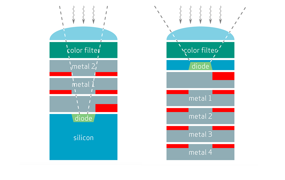
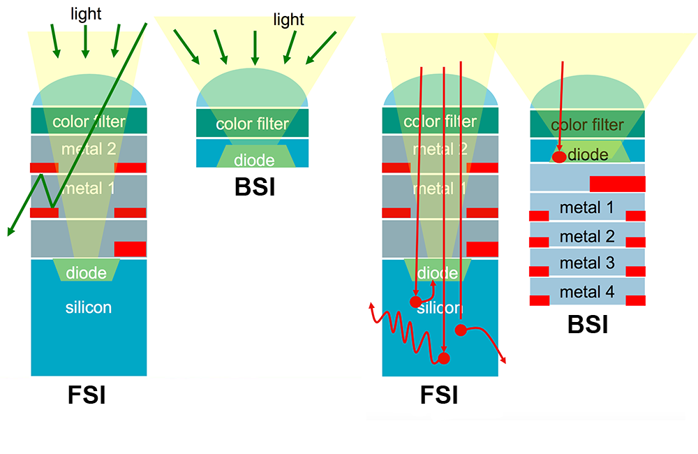
It’s clear that larger pixels generally lead to better image quality, but the structure of the sensor affects image quality as well. Conventional chips are built by layering metal and other materials on top of a silicon substrate or wafer. The first CMOS sensors were built this way as well; the circuitry and metal wires were layered on top of the photoactive silicon region. This frontside-illuminated (FSI) structure, where the light first passes through the circuitry and wiring before reaching the photoactive region of the pixel, is easy to manufacture but negatively affects image quality.
A pixel in an FSI CMOS sensor will have a quantum efficiency (QE), a measure of the number of incoming photons converted to electron-hole pairs, of less than 50% with narrowed spectrum coverage, because the layers above the pixel reflect and absorb a portion of the incoming light (QE can be as high as 80% when microlenses and light pipes are employed). In addition to reducing pixel sensitivity, reflected light also causes optical crosstalk, where a photon intended for one pixel gets bounced into an adjacent pixel instead, reducing image sharpness. This also reduces color accuracy, because green light may end up in a red pixel (adjacent pixels use different color filters). Electrical crosstalk, where electrons may leak into an adjacent pixel or get absorbed into the substrate, is another problem for FSI sensors due to their relatively thick silicon layer.
Placing the metal layers above the photoactive layer clearly degrades image quality, but it’s not the only downside. The FSI senor’s upper layers form an optical tunnel that restricts each pixel’s field of view, only admitting light rays below a specific angle of incidence, which gets worse for smaller pixels. This places restrictions on the optical stack, limiting the camera’s aperture diameter and requiring a thicker lens array.
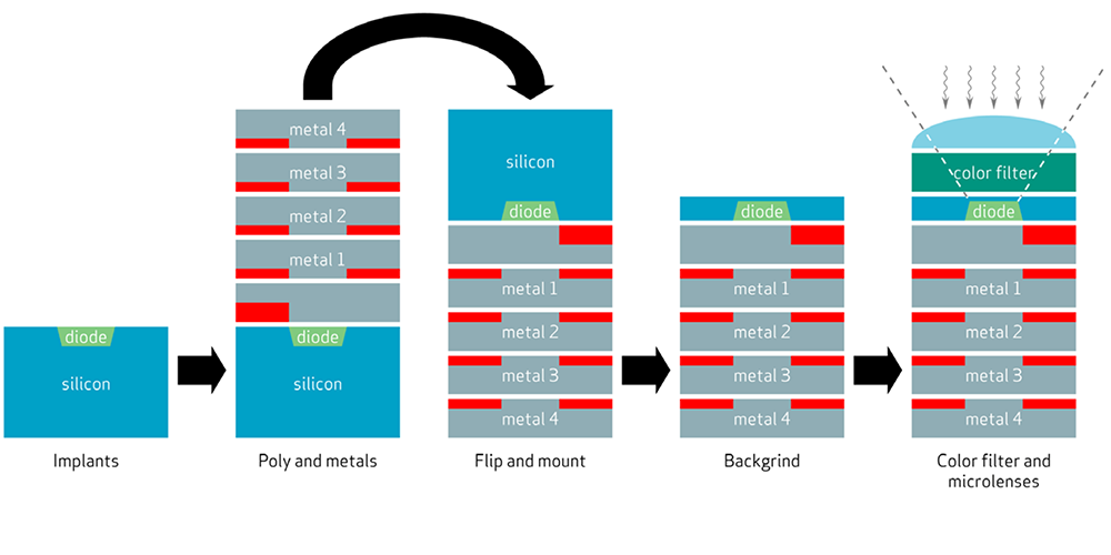
In 2007, OmniVision Technologies helped pioneer a new fabrication process to overcome these limitations. After creating the circuitry and metal interconnect layers, the back of the wafer is ground away until only a thin photoactive layer remains. This thinning process is necessary because visible light penetrates only a short distance into silicon. The chip is then used upside down, with light hitting the exposed photoactive layer on the backside directly. By placing the circuitry and metal below, where it cannot block or interfere with the incoming light, the backside-illuminated (BSI) CMOS sensor improves QE to over 90%, captures a wider spectrum of light, and reduces optical crosstalk. The BSI sensor can also capture a wider cone of light, which reduces the thickness of the lens array, allows for wider aperture lenses, and more flexibility for zoom lenses.
The BSI sensor’s thinner substrate also helps improve performance by reducing dark leakage current, where electrons leak out of the pixel well and into the substrate. Manufacturers also employ various means to limit electrical crosstalk. Samsung’s ISOCELL technology, for instance, uses a special material to construct a physical barrier between adjacent pixels, reducing electrical crosstalk by approximately 30%, according to Samsung.
Despite their higher cost, a consequence of the more complicated fabrication process, BSI sensors are now widely used in smartphones and tablets. Sony introduced its Exmor R series of BSI sensors in 2009, and Apple’s iPhone 4 and HTC’s EVO 4G, both released in 2010, became two of the first smartphones to use a BSI sensor for their rear camera. Other manufacturers of CMOS image sensors, such as Samsung and Toshiba, have also joined the BSI bandwagon.
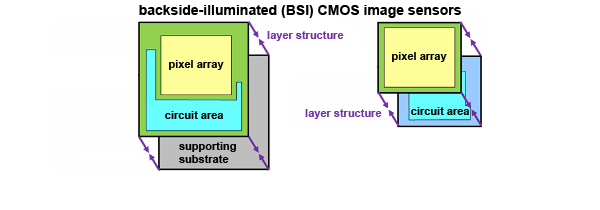
Looking to increase resolution and improve imaging performance, manufacturers are now moving to 3D or stacked layer BSI designs. Sony’s Exmor RS sensors were the first to employ this new technique, which moves the transistors from the photoactive layer onto one or more separate layers connected together by through-silicon vias (TSVs). This increases the die space available for photon sensing pixels, while simultaneously allowing for greater on-chip processing capabilities.
-
wtfxxxgp ReplyThanks for the informative article. You might have just cured my insomnia.
Geez. That was a cruel comment! hahaha
Seriously though, that article was very informative for those of us who like to know a bit about everything :) -
David_118 Great article. Very Informative. It would be useful, knowing these concepts, if there was a studio that took mobile cameras and used them on some standard set of scenes, either photographing paper with test patterns, or constructed scenes in low light, or whatever, that could measure things like signal-to-noise, HDR performance, optical abberations, shutter speed, etc. Anyone know of such an outfit?Reply -
MobileEditor ReplyGreat article. Very Informative. It would be useful, knowing these concepts, if there was a studio that took mobile cameras and used them on some standard set of scenes, either photographing paper with test patterns, or constructed scenes in low light, or whatever, that could measure things like signal-to-noise, HDR performance, optical abberations, shutter speed, etc. Anyone know of such an outfit?
There are several labs, such as DxOMark, Image Quality Labs, and Sofica, that perform these tests. We're considering adding some of these tests to our reviews, but they require expensive equipment and software to do it right. Hopefully, we'll be able to expand our camera testing in the future--budget and time permitting.
- Matt Humrick, Mobile Editor, Tom's Hardware -
zodiacfml Good job. Finally, someone who really knows about what's being written. The tone and some information though might be too much for someone who has not even heard of shutter speeds or aperture. I also feel there's information overload as each topic/headline deserves its own article including investigation on megapixel/resolution spec.Reply
