Chinese scientists claim carbon nanotube transistor breakthrough — AI performance boosts from Gate All Around design
GAA is here, but what about production node?

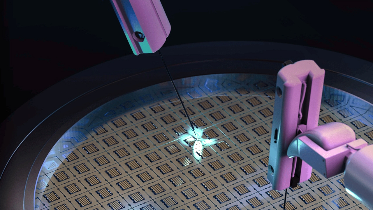
It is close to impossible to get into a Chinese semiconductor laboratory, but Chinese scientists are inclined to share the results of their work. Thus, our colleagues from TechXplore have found a paper from researchers at Peking University who claim to have built the industry's first tensor processing unit (TPU) featuring carbon nanotube transistors.
Before we go into what was achieved, let us talk a bit about carbon nanotube transistors and why they are important. Carbon nanotube (CNT) transistors are essentially gate-all-around (GAA) field-effect transistors (GAA FETs) that can be applied to pretty much everything, and have all the things that one expects from a GAA transistor such as enhanced control over performance and power and reduced leakage currents. Samsung has been using GAAFETs with its 3nm-class process technologies for a while, but so far this production node has been used for fairly simple cryptocurrency mining chips. Intel uses GAA FETs for CPUs made on its 20A node, while TSMC will adopt GAA transistors with its N2 process technology that will enter mass production in the second half of 2025.
Using this process technology featuring CNTs or GAAFETs, the researchers from Peking University built a small TPU, the world's first tensor processing unit featuring this type of transistors.
"We report a tensor processing unit (TPU) that is based on 3,000 carbon nanotube field-effect transistors and can perform energy-efficient convolution operations and matrix multiplication," the description of the paper published by Nature reads. "The TPU is constructed with a systolic array architecture that allows parallel 2-bit integer multiply–accumulate operations."
A five-layer convolutional neural network using this TPU can achieve up to 88% accuracy in MNIST image recognition while consuming only 295 µW of power. This is made possible by an optimized nanotube fabrication process that ensures a semiconductor purity of 99.9999% and ultra-clean surfaces, resulting in transistors with high on-current densities and consistent performance. System-level simulations suggest that an 8-bit TPU built with nanotube transistors at a 180 nm technology node could operate at a main frequency of 850 MHz and achieve an energy efficiency of 1 tera-operations per second per watt.
The researchers believe that the TPU's performance could be further improved. By fine-tuning the alignment of GAA FETs, reducing the size of transistors, and increasing the processing unit's bit capacity, the chip's efficiency and computational power could be enhanced even further, it is thought. Integrating the TPU with complementary metal-oxide-semiconductor (CMOS) logic is another avenue for potential improvement.
Keeping in mind that we are talking about GAA FETs implemented using a 180 nm-class process technology, the practical applicability of this TPU is low, to say the least. However, using a working TPU circuit, researchers can now refine process technology, which is utterly important for further development of Chinese semiconductor capability.
Get Tom's Hardware's best news and in-depth reviews, straight to your inbox.

Anton Shilov is a contributing writer at Tom’s Hardware. Over the past couple of decades, he has covered everything from CPUs and GPUs to supercomputers and from modern process technologies and latest fab tools to high-tech industry trends.
-
bit_user Reply
Research tends to happen on much older nodes. The two key questions are:The article said:Keeping in mind that we are talking about GAA FETs implemented using a 180 nm-class process technology, the practical applicability of this TPU is low, to say the least.
How do the CNT compare to similar CMOS transistors, on the same node?
How well do they think the CNT will scale down to modern production nodes, both in terms of performance and manufacturability?