First functional graphene semiconductor paves the path to post-silicon chips — Georgia Tech researchers' material can be used with standard chipmaking methods

Epitaxial graphene bonded to silicon carbide
(Image credit: Georgia Tech)

Georgia Tech researchers claim they have created “the world’s first functional semiconductor made from graphene.” Importantly, the research team’s epitaxial graphene is claimed to be compatible with conventional microelectronics processing methods and is thus a realistic silicon alternative. Moreover, this refined material achieves a desirable band gap for electronics applications and has latent potential for future quantum computing devices.

Technology pundits have highlighted the battle to keep Moore’s Law alive for years. One of the key issues faced by those wanting to push semiconductors forward is that silicon is reaching its limits. Graphene has consistently been touted as a wonder material (ever since its discovery in 2004). Still, it has not yet been instrumental to any significant or widely adopted technological breakthrough(s). However, the Georgia Institute of Technology researchers seem to be onto something big with their refined epitaxial graphene bonded to silicon carbide.

(Image credit: Georgia Tech)

To get to this point, Dr. Walter de Heer, Regents’ Professor of Physics at Georgia Tech, led a team of researchers based in Atlanta and Tianjin, China. The professor has been working on 2D graphene since the early 2000s.

“We were motivated by the hope of introducing three special properties of graphene into electronics,” he said. “It's an extremely robust material, one that can handle very large currents, and can do so without heating up and falling apart.”

Despite those three properties, a key semiconductor characteristic has been absent from graphene-based materials until now. “A long-standing problem in graphene electronics is that graphene didn’t have the right band gap and couldn’t switch on and off at the correct ratio,” said Dr. Lei Ma, de Heer’s co-founder of the Tianjin International Center for Nanoparticles and Nanosystems at Tianjin University in China. “Over the years, many have tried to address this with a variety of methods. Our technology achieves the band gap, and is a crucial step in realizing graphene-based electronics.” Lei Ma was also the co-author of the Ultrahigh-mobility semiconducting epitaxial graphene on silicon carbide paper published by Nature today.

(Image credit: Georgia Tech)

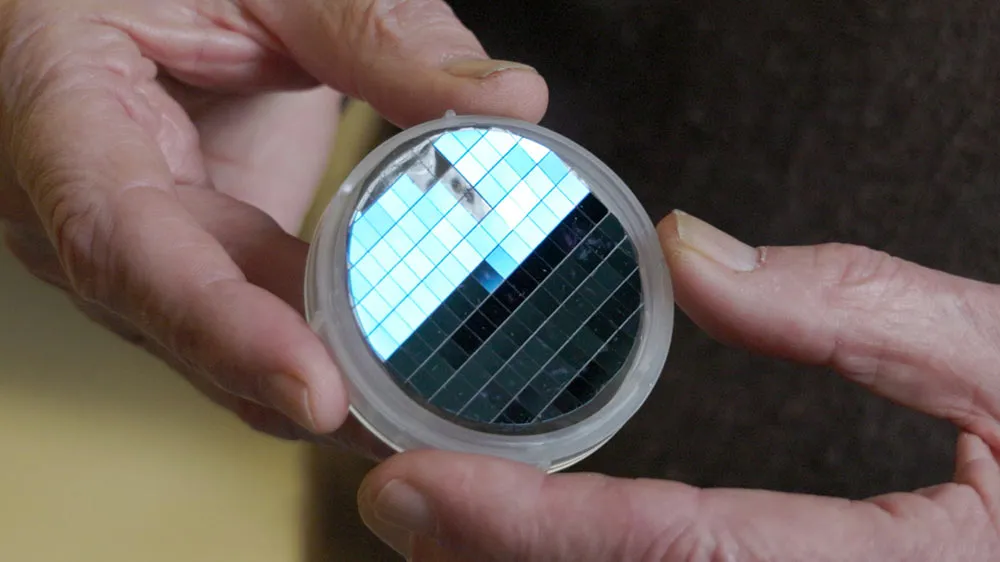
The research team’s breakthrough came as they successfully learned how to grow graphene on silicon carbide wafers using special furnaces – producing epitaxial graphene bonded to silicon carbide. According to the Georgia Tech blog, it took a decade to perfect this material. Now, tests show their graphene-based semiconductor material has ten times greater mobility than silicon. “In other words, the electrons move with very low resistance, which, in electronics, translates to faster computing,” explained the educational and research establishment’s blog.

The Regents' Professor of Physics puts the appealing properties of graphene-based electronics in simpler terms. “It's like driving on a gravel road versus driving on a freeway,” de Heer said of the electron movement through his refined graphene semiconductor material. “It's more efficient, it doesn't heat up as much, and it allows for higher speeds so that the electrons can move faster.”

According to the Georgia Tech research team, their epitaxial graphene bonded to silicon carbide is far superior to any other 2D semiconductors in development. Prof de Heer characterized the semiconductor materials breakthrough as a “Wright brothers moment” and also highlighted the material’s compatibility with the quantum mechanical wave properties of electrons, meaning it could be instrumental to future advances in quantum computing.

Mark Tyson
Freelance News Writer

Mark Tyson is a Freelance News Writer at Tom's Hardware US. He enjoys covering the full breadth of PC tech; from business and semiconductor design to products approaching the edge of reason.

  • Crazyy8
    But does it perform well? It may function, but who knows if it will outperform standard chips.
    Reply
  • bit_user
    Crazyy8 said:
    But does it perform well? It may function, but who knows if it will outperform standard chips.
    That's the idea. By improving signal propagation speed and reducing heat, my guess is they expect it can run at higher clock speeds, within the same power envelope.

    Keep in mind that they only made a proof of concept to show the technology can work. Presumably, the next step would be to try and fab some fundamental logic gates on it, at which point there will hopefully be more concrete projections of the expected benefits.
    Reply
  • TCA_ChinChin
    bit_user said:
    Keep in mind that they only made a proof of concept to show the technology can work. Presumably, the next step would be to try and fab some fundamental logic gates on it, at which point there will hopefully be more concrete projections of the expected benefits.
    I'm cautiously optimistic, but I imagine that even if the next steps are easily feasible, I can see another decade of research before more papers/technical breakthroughs are achieved. I feel like so many breakthroughs/research based off of graphene have taken so long to mature, it feels like a nuclear fusion scenario, where even if real tangible progress is made every year, the timeline to actual commercial use is forever in limbo.
    Reply
  • bit_user
    TCA_ChinChin said:
    I feel like so many breakthroughs/research based off of graphene have taken so long to mature, it feels like a nuclear fusion scenario, where even if real tangible progress is made every year, the timeline to actual commercial use is forever in limbo.
    I think that's because it's hard to form large, continuous sheets of it, and its properties are orientation-dependent. So, I think that means you pretty much have to form it in-place, rather than somehow manufacture and apply it as separate steps.

    In this case, graphene wasn't up to the task, all by itself. So, there was the added dimension of how to workaround that. Then, once you have a theory, you have to figure out how to fabricate the hybrid material.
    Reply
  • LuxZg
    "Tianjin University in China" -> oh no, they have already stolen the designs! ;-)

    "Walter de Heer, Regents’ Professor of physics at Georgia Tech, led a team of researchers based in Atlanta, Georgia, and Tianjin, China, to produce a graphene semiconductor that is compatible with conventional microelectronics processing methods — a necessity for any viable alternative to silicon."

    "Over the next decade, they persisted in perfecting the material at Georgia Tech and later in collaboration with colleagues at the Tianjin International Center for Nanoparticles and Nanosystems at Tianjin University in China. De Heer founded the center in 2014 with Lei Ma, the center’s director and a co-author of the paper."

    Need to save these quotes for discussions another 10 years down the line when everyone start spreading FUD...

    Anyway, back to news reading. This is real interesting, but same as bunch of other tech will take a lot more time to actually show up in everyday devices like PCs, phones, cars... Hope I'm still alive when it happens! (not that it will take THAT long, but I'm also not young anymore)
    Reply
  • vehekos
    Graphene cannot preserve Moore's law, because it cannot be miniaturized much. It needs a lot of atoms just to be graphene.
    Reply
  • bit_user
    vehekos said:
    Graphene cannot preserve Moore's law, because it cannot be miniaturized much. It needs a lot of atoms just to be graphene.
    Like how many? Is 10 enough?

    Even if they do turn out to be bigger, that can probably be worked around by layering or stacking, since they run cooler.

    I think it's a mistake to second-guess them, especially given how much focus this area has gotten. If it really didn't have the potential for miniaturization to anywhere near leading edge nodes, I doubt they've have continued investigating it.
    Reply
  • DavidC1
    Yea, such "Wonder" material which will cause serious health issues down the road since practically every area is trying to use nano tech and graphene including and not limited to waterproof coating, antibacterial lining, and paint. The material breaks off similar to flint meaning sharp and long and the micro structures will easily be carried off into the wind into your lungs and other systems.

    Use it for CPUs and forget everything else please.
    Reply
  • bit_user
    DavidC1 said:
    Yea, such "Wonder" material which will cause serious health issues down the road since practically every area is trying to use nano tech and graphene including and not limited to waterproof coating, antibacterial lining, and paint.
    That has nothing to do with this. A CPU is not going to leak out nanoparticles of anything.

    DavidC1 said:
    The material breaks off similar to flint meaning sharp and long and the micro structures will easily be carried off into the wind into your lungs and other systems.
    Well, it's ultimately just carbon. So, it will eventually react with other elements in the environment, as opposed to staying like that.

    Sure, the health & environmental implications of putting nanoparticles of anything into various products needs to be understood and managed, but I wouldn't single out graphene, here.
    Reply
  • The Beav
    vehekos said:
    Graphene cannot preserve Moore's law, because it cannot be miniaturized much. It needs a lot of atoms just to be graphene.
    Moore's law is already slowing down with traditional silicon, we're getting close to single atom separation now with 2nm, and there's also a very large interference issue that's cropped up and stopping further miniaturization. So Moore's law will essentially stop, or slow down, unless other avenues of miniaturization are explored. If the atoms in graphene are smaller than those in silicon this could be a huge advantage in miniaturization.
    Reply