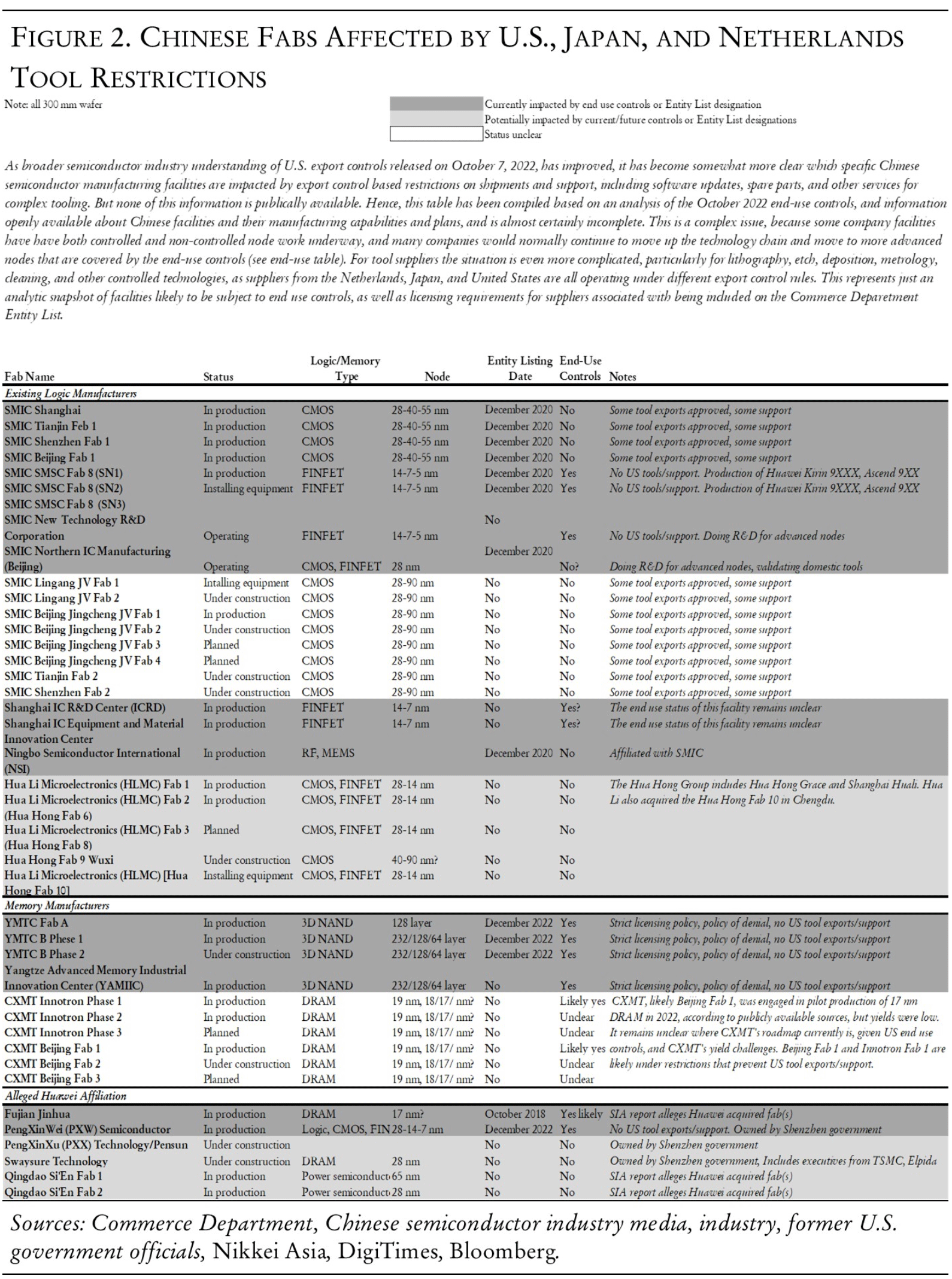
The U.S. has sanctioned 18 Chinese fabs, dozens remain in white zone
China has big plans for semiconductor industry and they include self reliance.

China's semiconductor industry has faced major challenges due to intensified U.S. export controls, particularly targeting blacklisted companies like SMIC, YMTC, and CXMT. However, even SMIC and CXMT can still get the chipmaking equipment they need for fabs that use the so-called trailing nodes, reports American Affairs. The question is, how many of those tools end up in blacklisted fabs?
The restrictions imposed by two U.S. governments over the past six years aim to prevent Chinese firms from advancing in cutting-edge semiconductor fabrication processes, as the latter can be used to make chips that will boost China's military capabilities. Of course, in response, China has accelerated efforts to develop domestic chipmaking equipment capabilities and reduce reliance on foreign tools. But do the imposed restrictions work?
Sweeping controls
The Biden administration's export controls, updated significantly in October 2022 and October 2023, focus on restricting China's access to advanced chipmaking tools. These new laws specifically target leading-edge process technologies that rely on FinFET and gate-all-around (GAA) transistors, making it difficult for Chinese firms to progress in advanced semiconductor technology. The restrictions also include novel end-use controls and limitations on U.S. persons, adding to the challenges faced by China's domestic semiconductor industry.
In light of these constraints, Chinese chipmakers are collaborating with domestic WFE makers to develop and validate equipment, aiming to create production processes free from tools made in the Netherlands, Japan, and the U.S.
Cannot stop Chinese semiconductor industry
Despite these challenges, leading foundries like SMIC are focusing on expanding their capacities at mature nodes while leveraging available Western tools to sustain advanced node production. For example, SMIC is making progress with advanced processes and uses deep ultraviolet (DUV) tools (such as Twinscan NXT 2050i) for production at its 2nd generation 7nm process technology and reportedly a 5nm fabrication process using multi-patterning, despite the complexities that such a technique entails.
Just as it did several years ago, Chinese foundry champion SMIC is fostering public-private partnerships to build its fabs. There is a catch here: The U.S. government has no problems with SMIC operating fabs that make chips on 28nm – 90nm process technologies. These fabs are not sanctioned and American, Dutch, and Japanese companies can sell their tools to equip such fabs with no restrictions. The problem, however, is that SMIC can buy tools to equip its 'white list fabs' but then install those tools into more advanced fabs that are blacklisted, and it is pretty hard for the U.S. government to control the destination of tools shipped by companies to 'white list fabs.'
Meanwhile, the Chinese government is easing the transfer of state-backed research and development to private-sector companies, encouraging collaboration to overcome technological bottlenecks. This strategy involves funding and facilitating multiple teams to tackle critical issues of leading-edge 7nm and 5nm-class process technologies. This approach is similar to successful approaches in other sectors like exascale computing, something that the U.S. government is trying to slow down, if not stop.
Get Tom's Hardware's best news and in-depth reviews, straight to your inbox.
The Chinese industry is also concentrating on building domestic alternatives across various sectors, including electronic design automation (EDA) tools, advanced materials, and packaging techniques. Efforts to develop a self-reliant semiconductor ecosystem are gaining momentum, with companies working on key technologies such as multi-chiplet designs and 2.5D and 3D back-end packaging technologies. These efforts are crucial for improving performance levels and bridging to new, domestic-only production processes.
The current strategy includes both short- and long-term goals. In the short term, leading domestic foundry SMIC is said to be establishing 40nm and 28nm production lines free of U.S. equipment. Meanwhile, Chinese toolmaker SMEE is working on lithography tools that are good enough for 28nm process technology, though it is unclear when the company can produce these tools in volume. The path forward involves progressing to 14/10nm and 7nm-class processes by 2025-2026.
In the longer term, China plans to develop extreme ultraviolet (EUV) lithography capabilities, which are required for 3nm and more advanced process technologies. Multiple coordinated efforts are underway to establish a complete ecosystem for EUV production processes, involving collaboration among research institutions, universities, and companies like Huawei. These efforts are crucial for achieving technological self-reliance and ensuring the sustainability of China's semiconductor industry.
Centralized oversight
China has established a new leading group under Vice Premier Ding Xuexiang to oversee semiconductor industry policy, signaling a shift towards a more centralized oversight model. Ding Xuexiang is not new to the semiconductor industry. He graduated with an engineering degree from the Northeast Heavy Machinery Institute in Qinghuangdao, now known as Yanshan University, in 1982. Then, he started his career at the Shanghai Research Institute of Materials (SRIM), where he worked from 1982 until 1999. During his tenure at SRIM, he rose through various research, administrative, and party-related roles.
This new strategy results from internal deliberations and a review of past approaches to semiconductor industry policy. The government is also increasing investment in basic research and development that is conducted by the government and one or two private companies. The results of such work are then transferred to the private sector.
Overall, the Chinese semiconductor industry is making significant efforts to build a self-reliant ecosystem amid ongoing U.S. export controls. The industry's future will depend on its ability to overcome technological challenges, validate domestic wafer fab equipment, and develop advanced manufacturing capabilities to produce new products with largely domestic supply chains.

Anton Shilov is a contributing writer at Tom’s Hardware. Over the past couple of decades, he has covered everything from CPUs and GPUs to supercomputers and from modern process technologies and latest fab tools to high-tech industry trends.
-
zsydeepsky it's a good report, comprehensive and up to date.Reply
by the way, Huawei's Hisilicon (Huawei's chip design department) is going to host its first announcement event in 9.9, roughly a month later. it's the first time since sanction for Huawei to showcase their new chips (they never showcased Kirin 9000s & Kirin 9010). I wonder what they will show, and what this move could indicate.
rumor says that they have achieved sanction-free, pure domestic manufacturing capability. might keep an eye on it. -
COLGeek Folks, please focus on the technology aspects of the article. If you have constructive input to improve the article, then politely post it so the author can take into consideration.Reply
Trolling anyone will not be tolerated, nor will off topic banter.
Thank you.
