DOE Enters Partnership to Use World's Largest Chips With 1.2 Trillion Transistors and 400,000 Cores
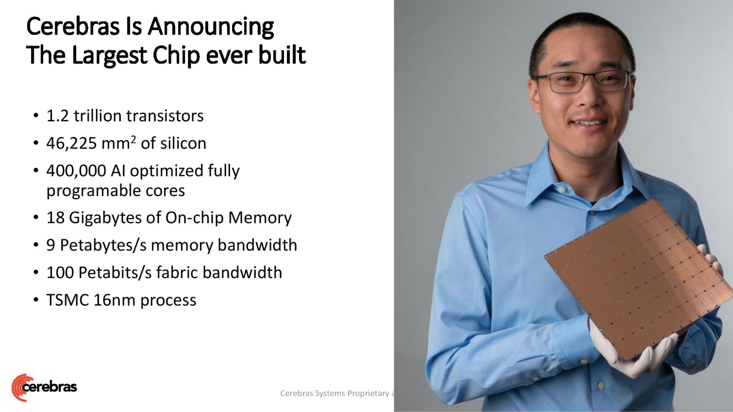
Cerebras Systems, makers of the world's largest single processor that weighs in with a whopping 1.2 trillion transistors and 400,000 AI cores, announced today that it has entered into a partnership with the Department of Energy (DOE), long the leader in the supercomputing space, to use its new wafer-scale chips for basic and applied science and medicine with super-scale AI.
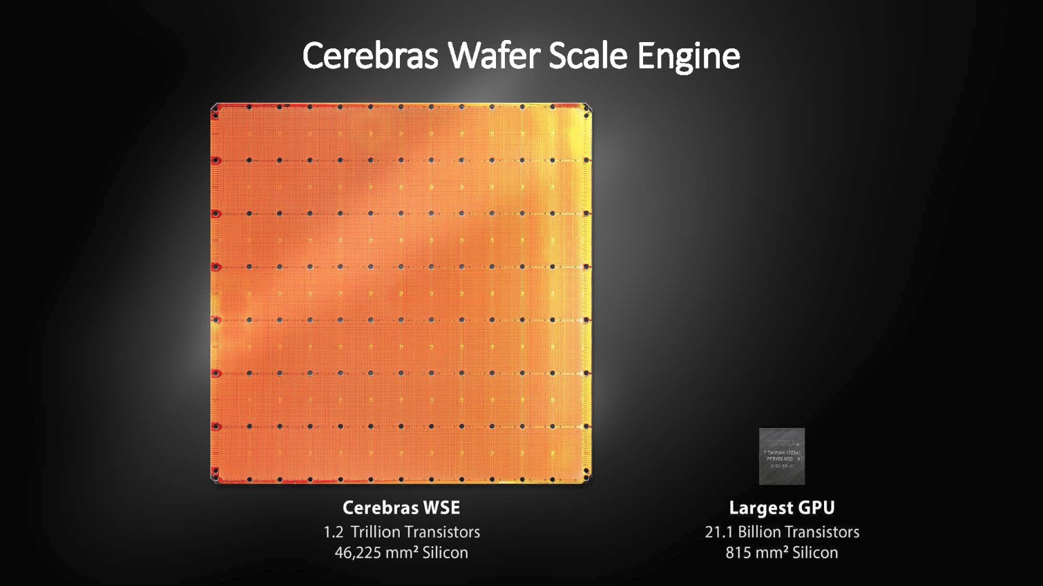
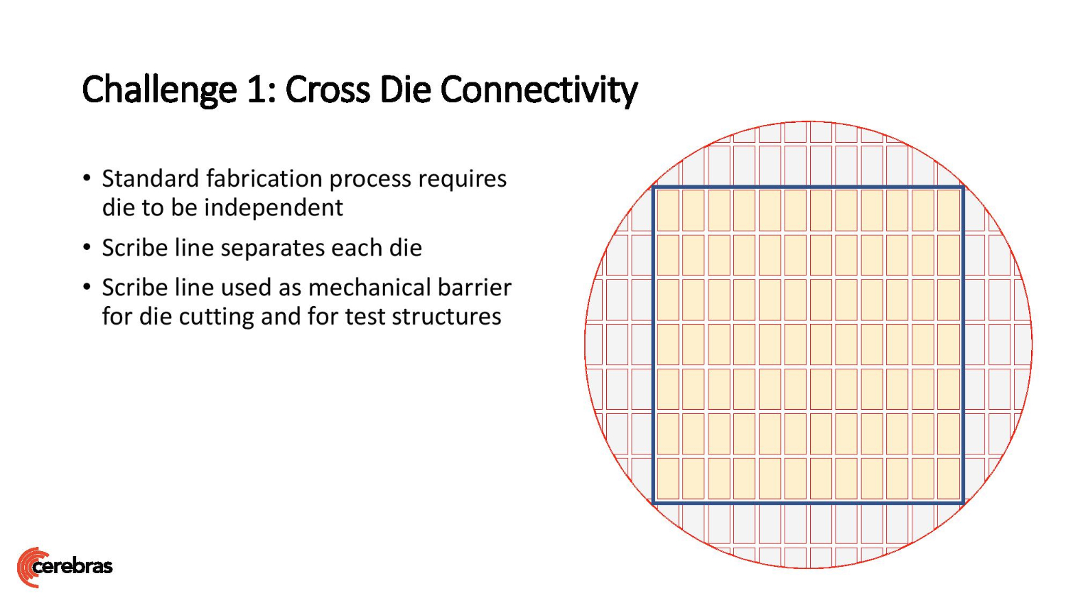
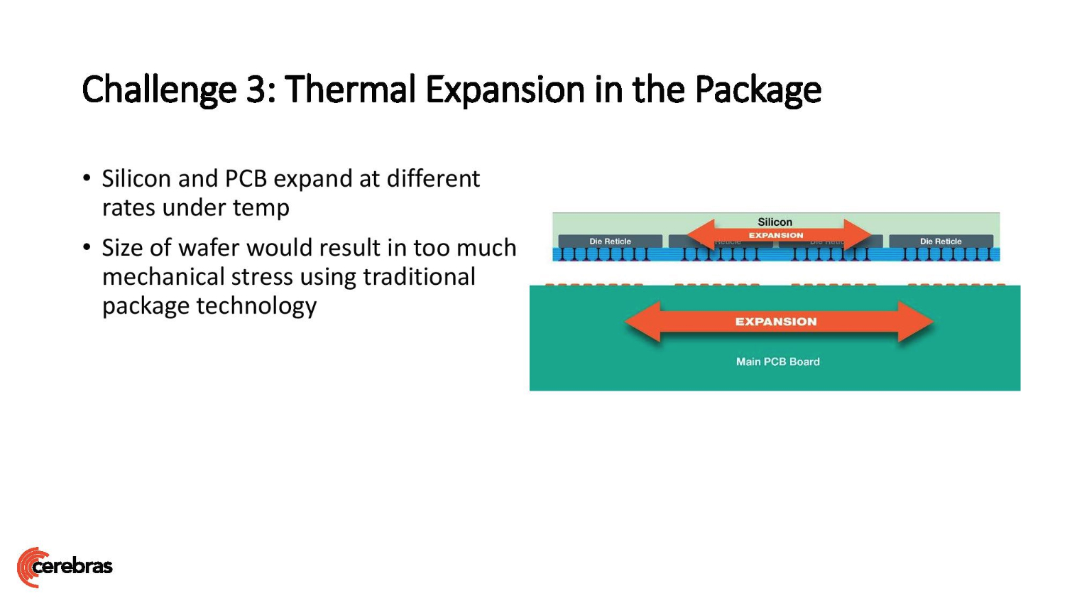
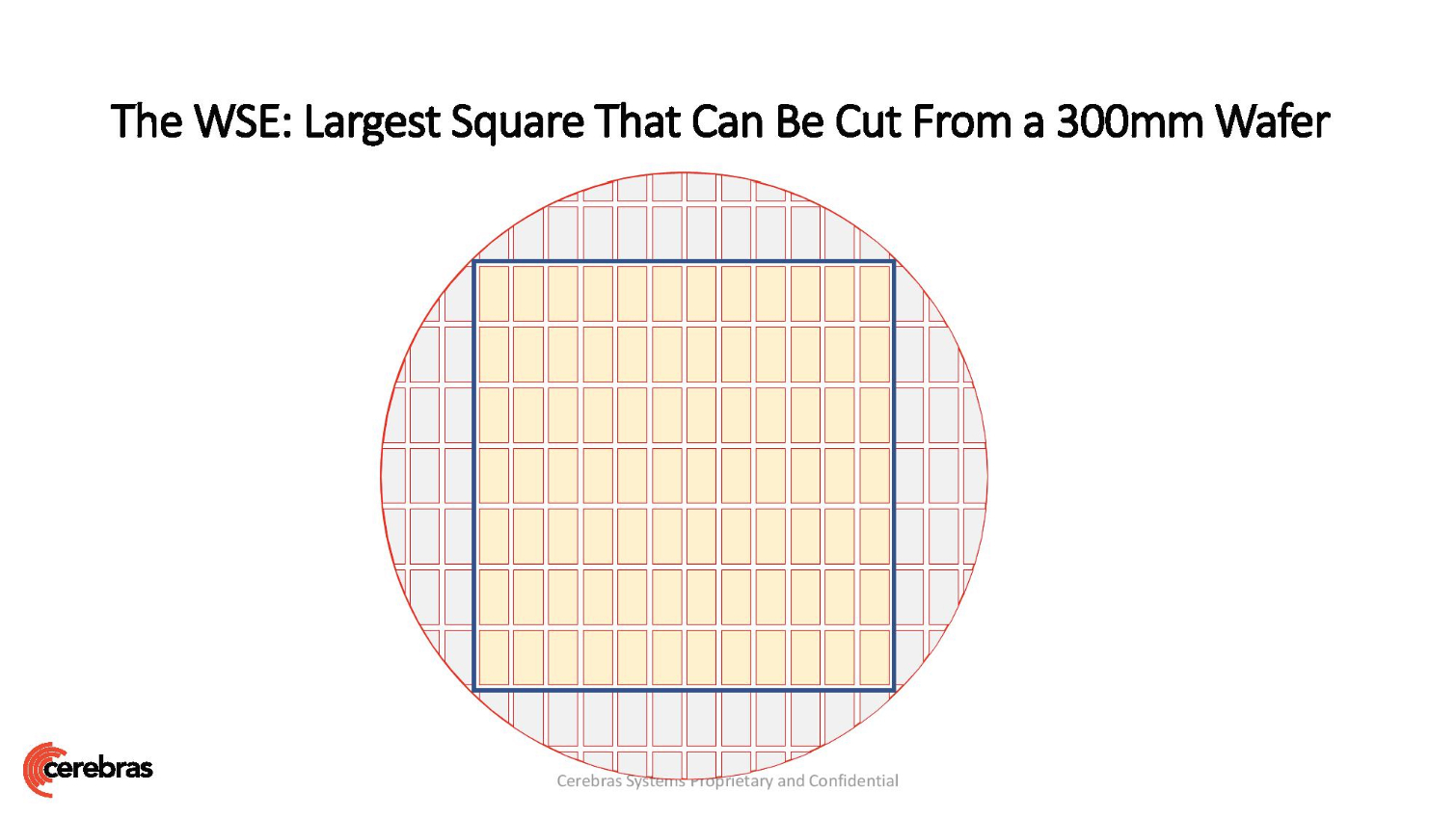
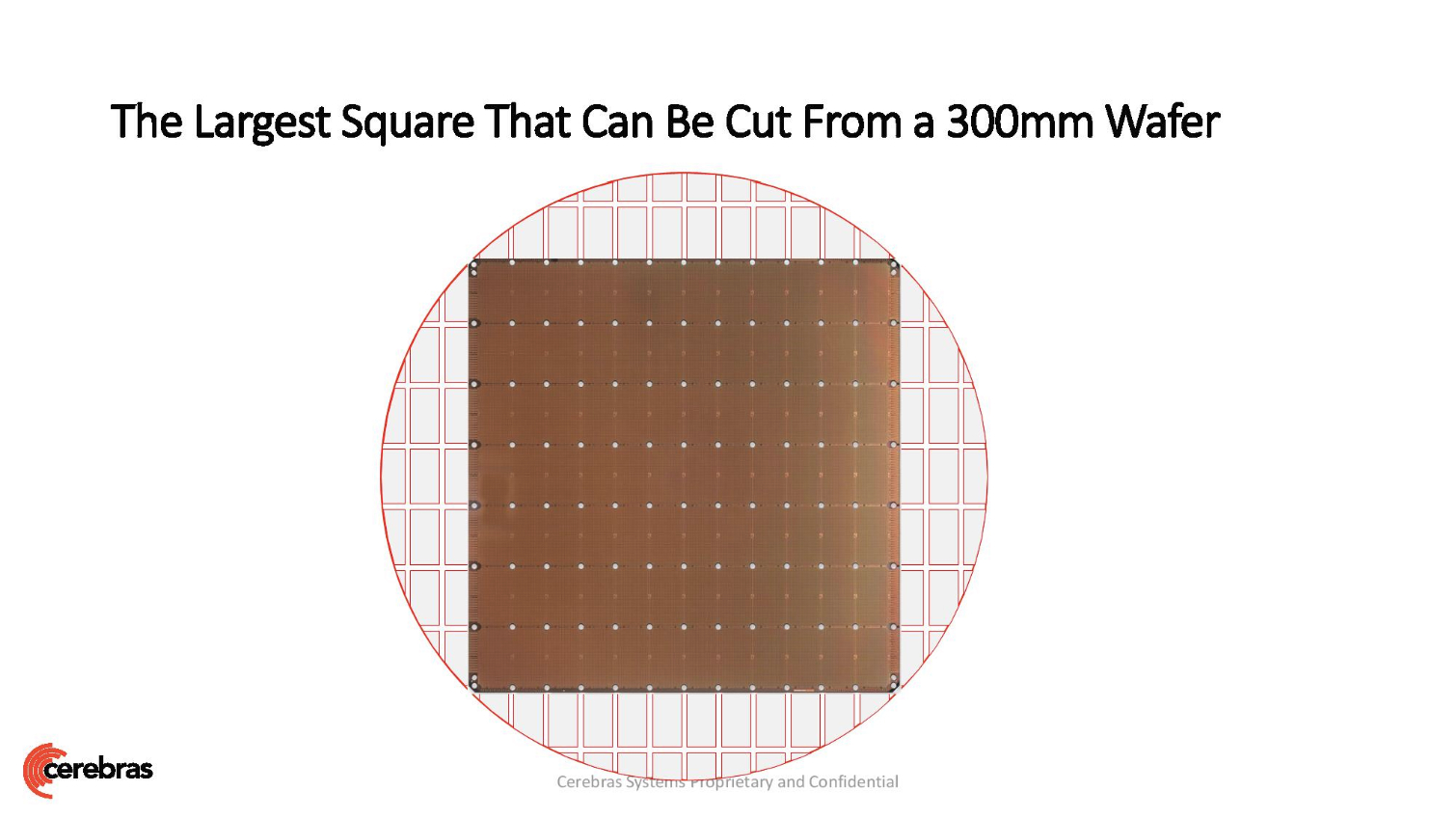
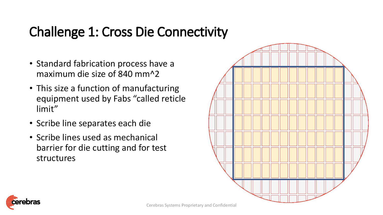
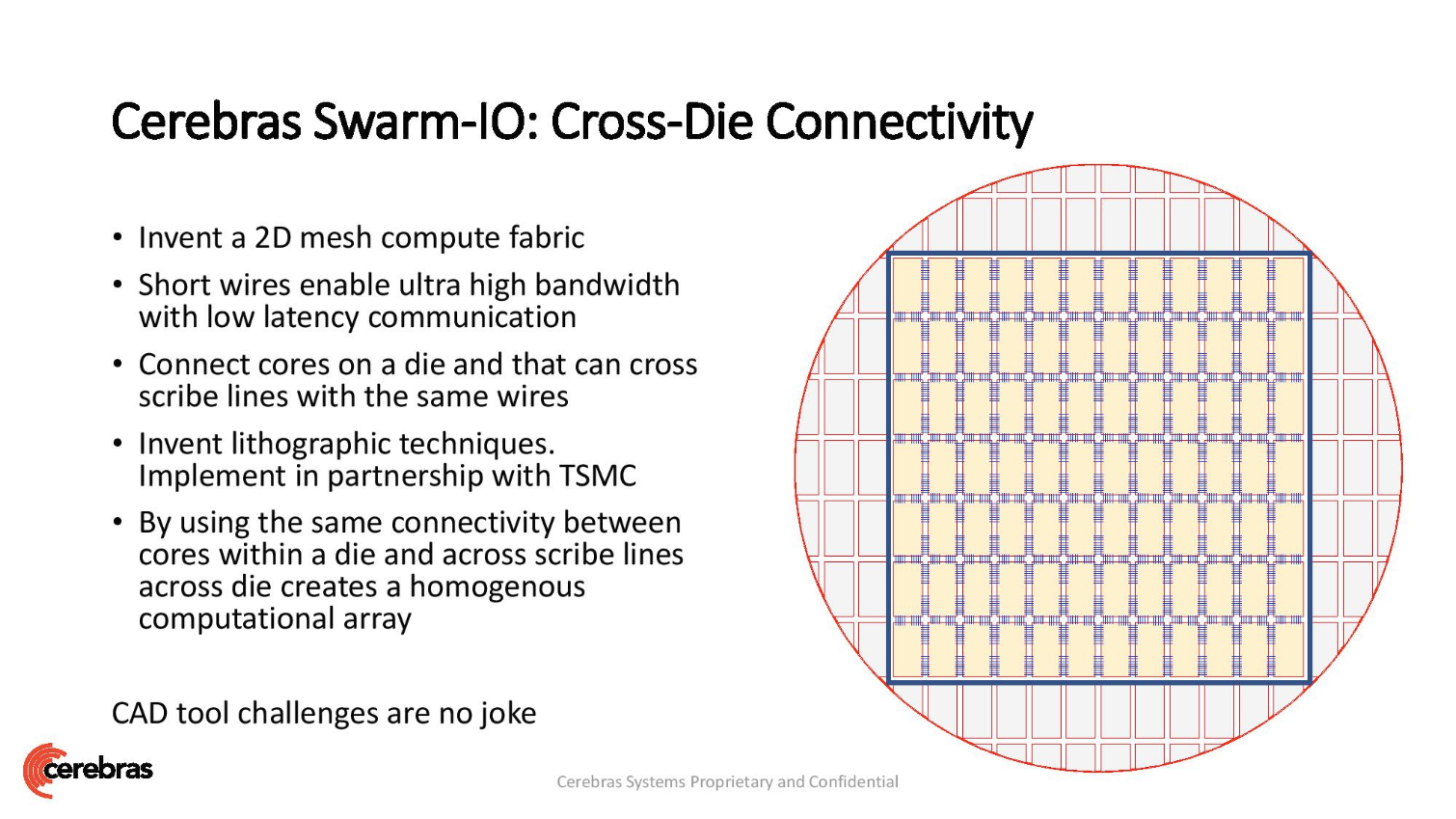
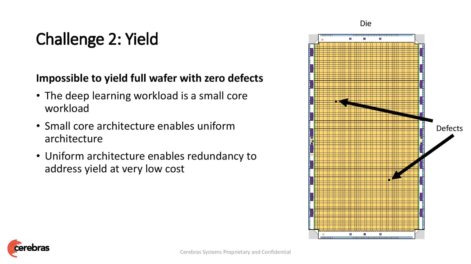
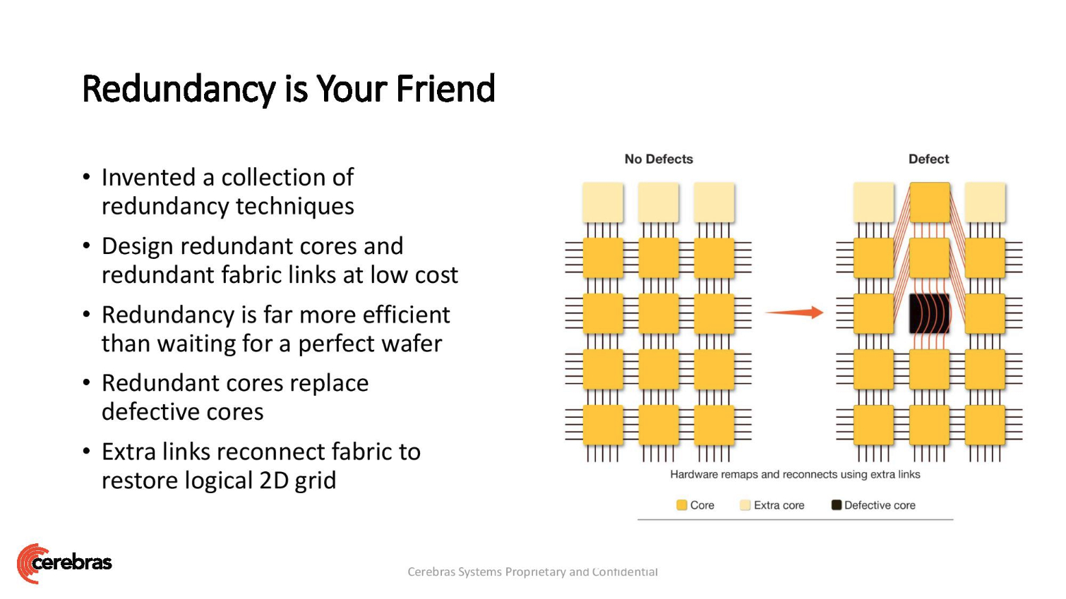
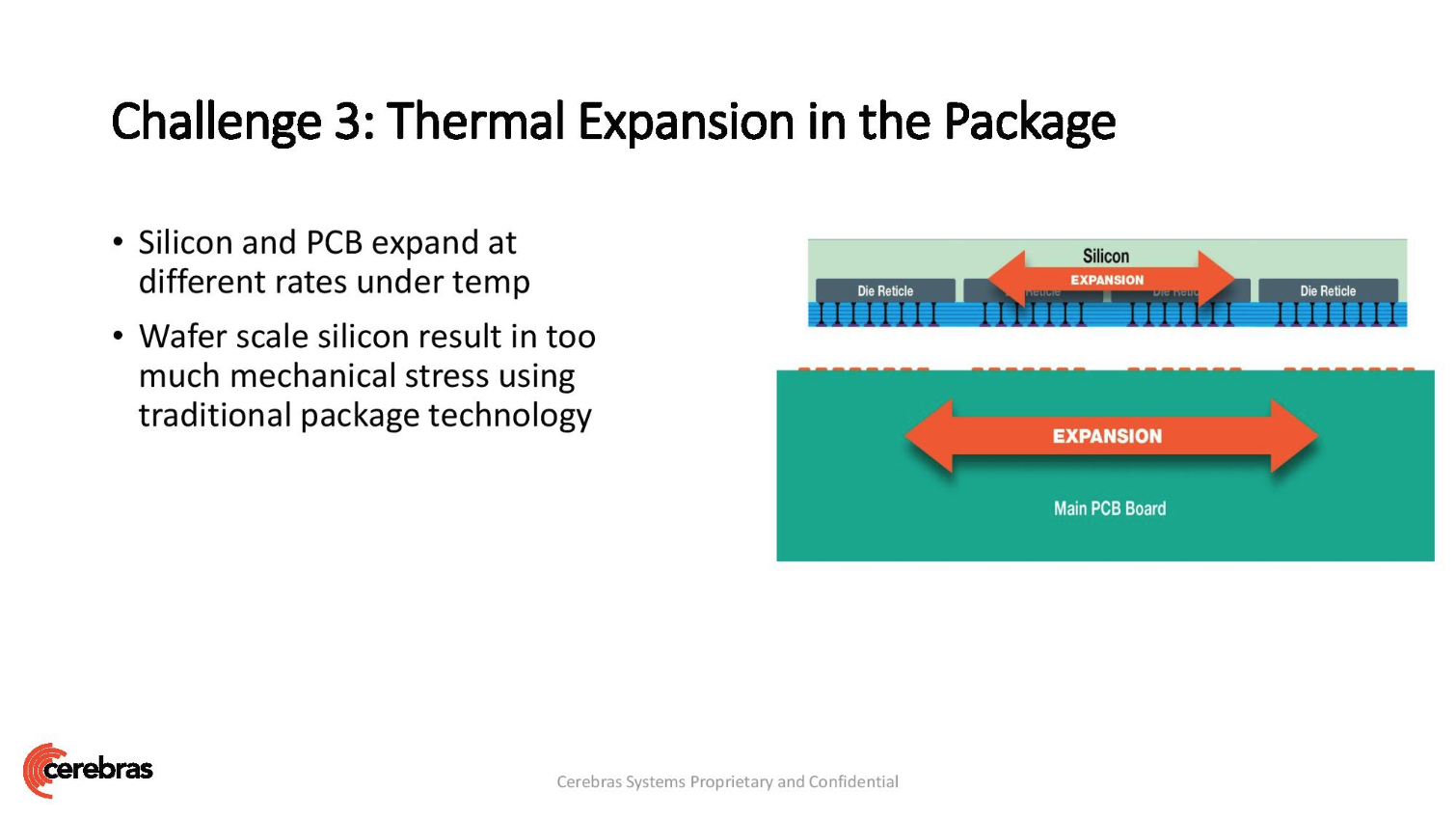
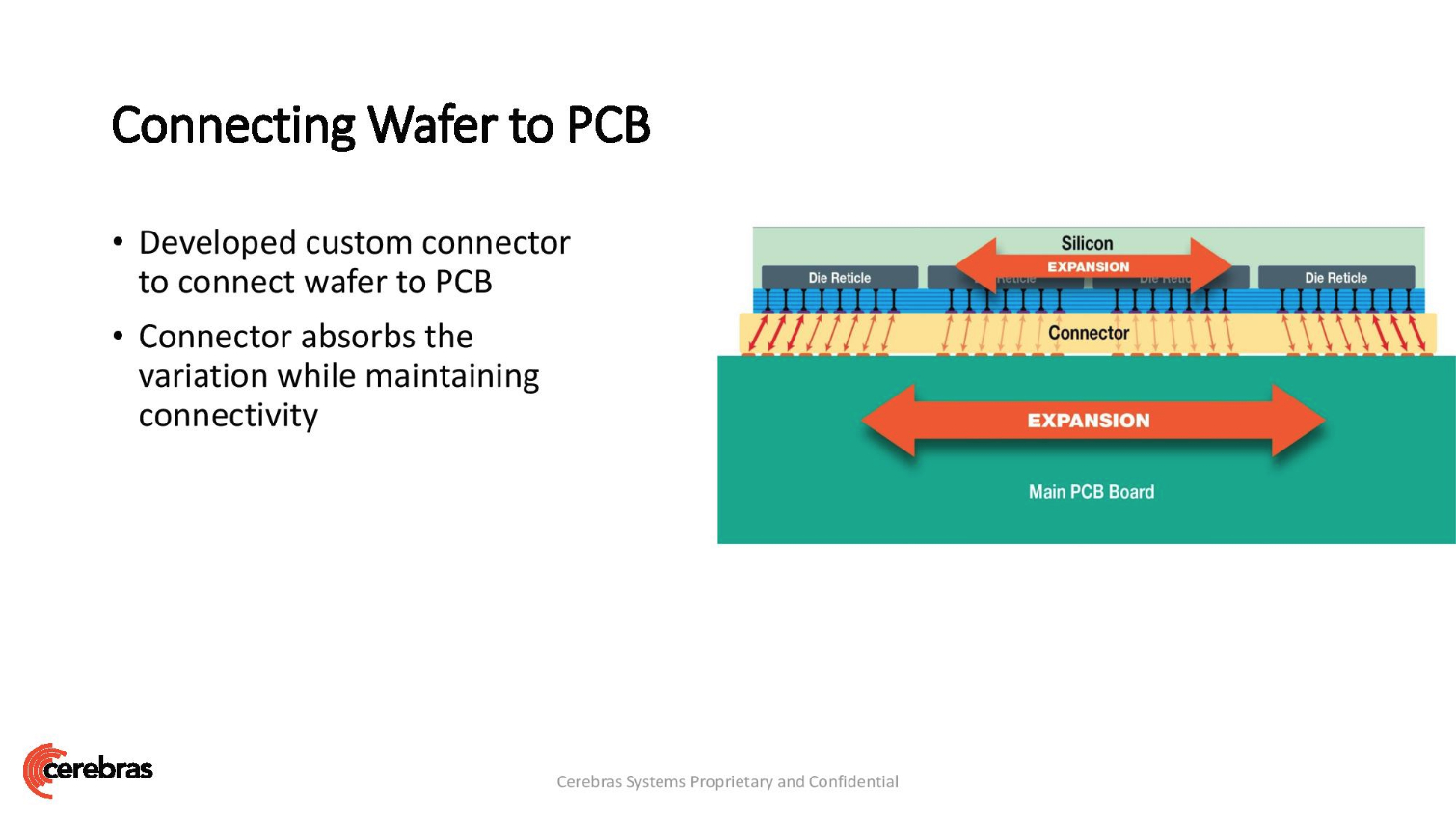
The Cerebras Wafer Scale Engine (WSE) sidesteps the reticle limitations of modern chip manufacturing, which limit the size of a single monolithic processor die, to create the wafer-sized processor. The company accomplishes this feat by stitching together the dies on the wafer, thus allowing it to work as one large cohesive unit.
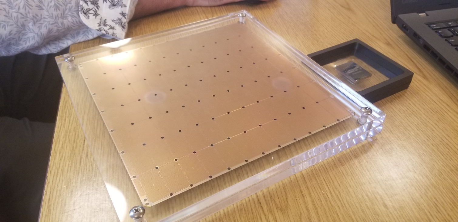
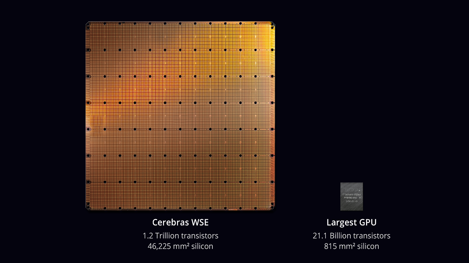
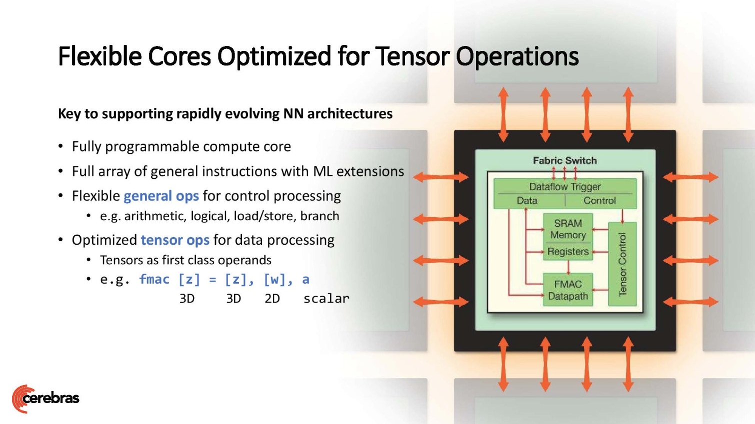
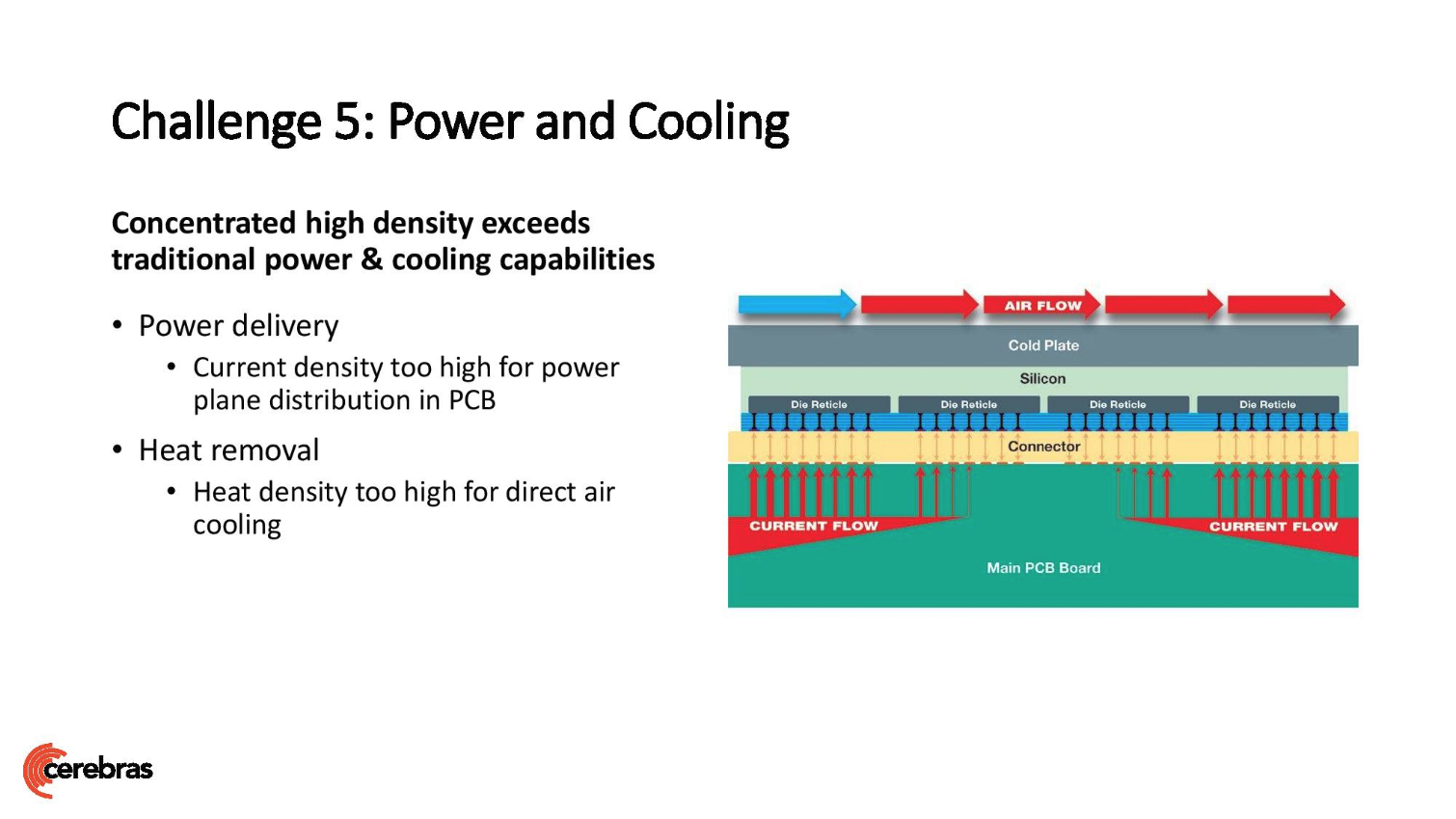
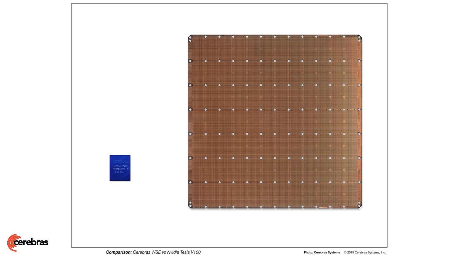
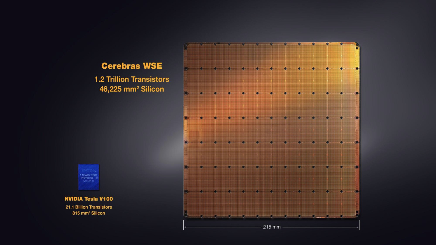
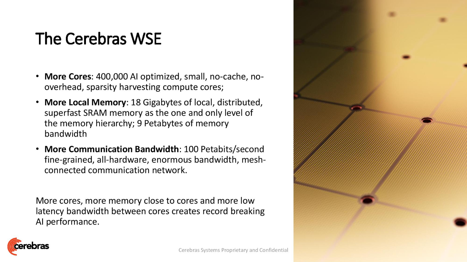
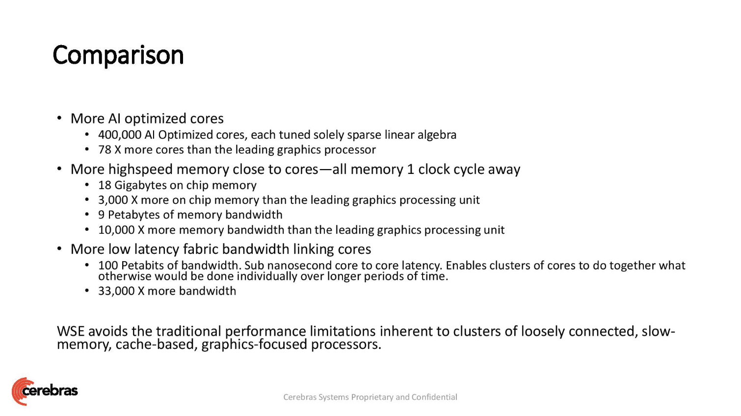
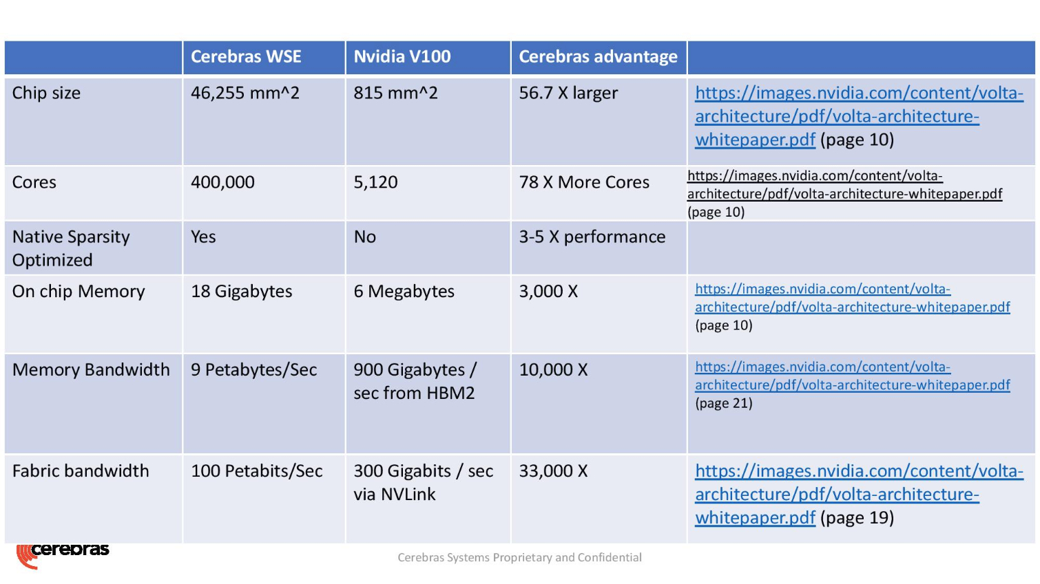
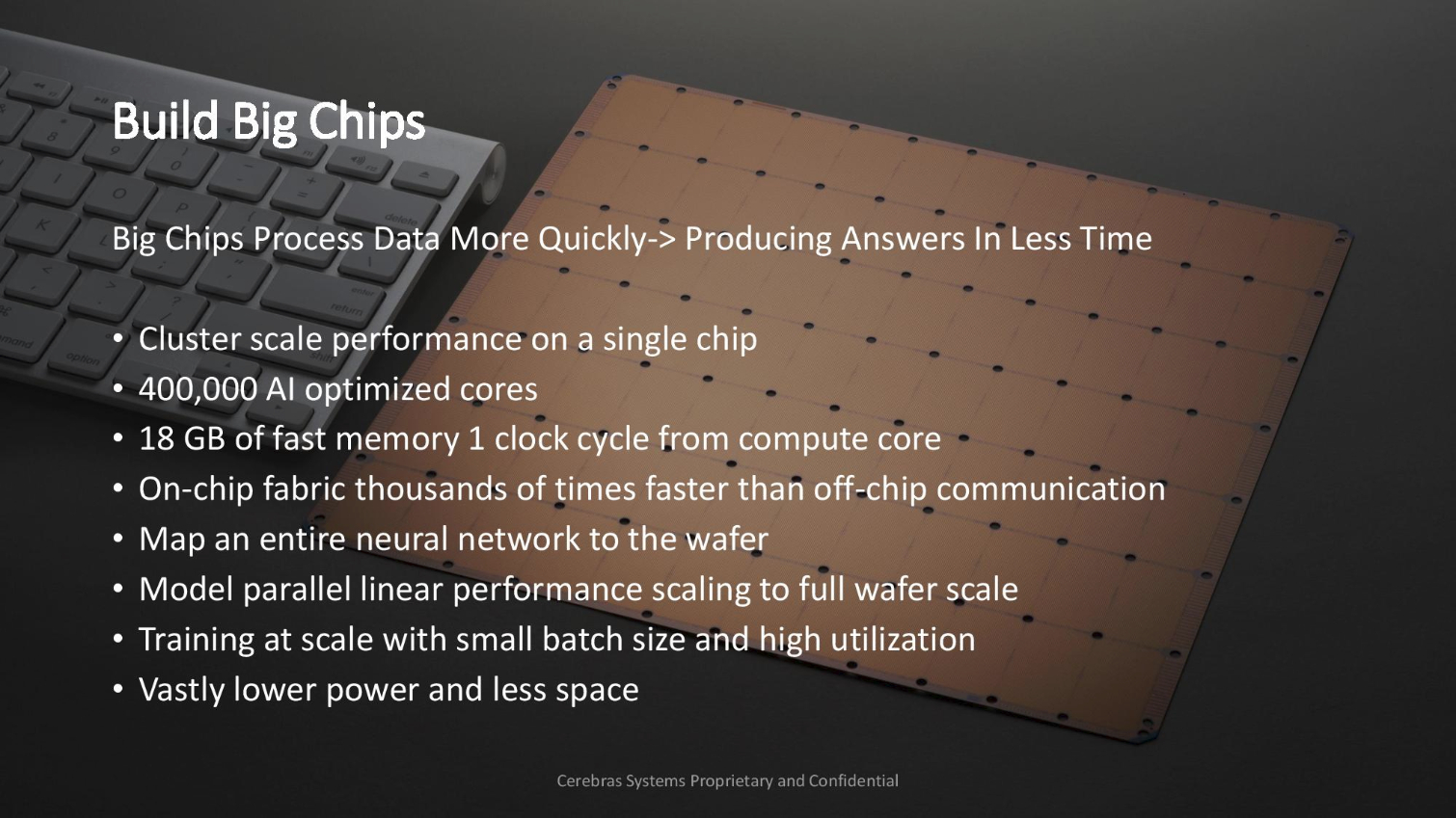
That creates a massive processor that measures 42,225 square millimeters, the largest in the world, that packs 1.2 trillion transistors fabbed on TSMC's 16nm process. That's 56.7 times larger than the world's largest GPU (815mm2 with 21.1 billion transistors). The massive chip also comes packing a whopping 40,000 AI-processing cores paired with 18GB of on-chip memory. That pushes out up to 9 PBps, yes, petabytes per second, of memory bandwidth. We recently had the chance to see the massive chip up close at the Hot Chips conference, and as you can see, it is larger than our laptop's footprint.
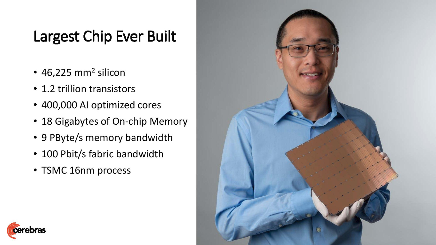

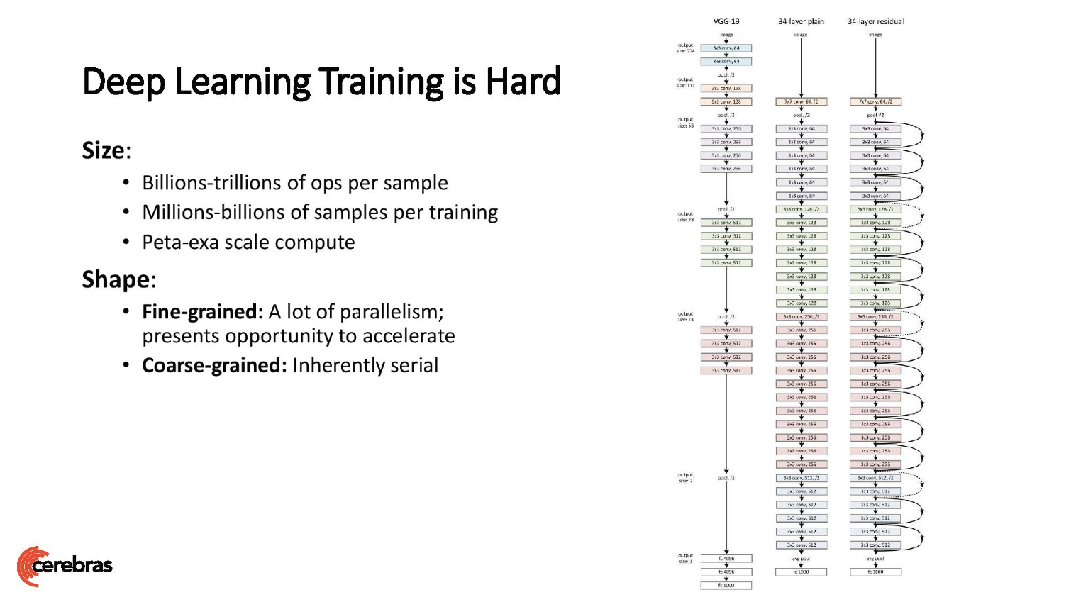


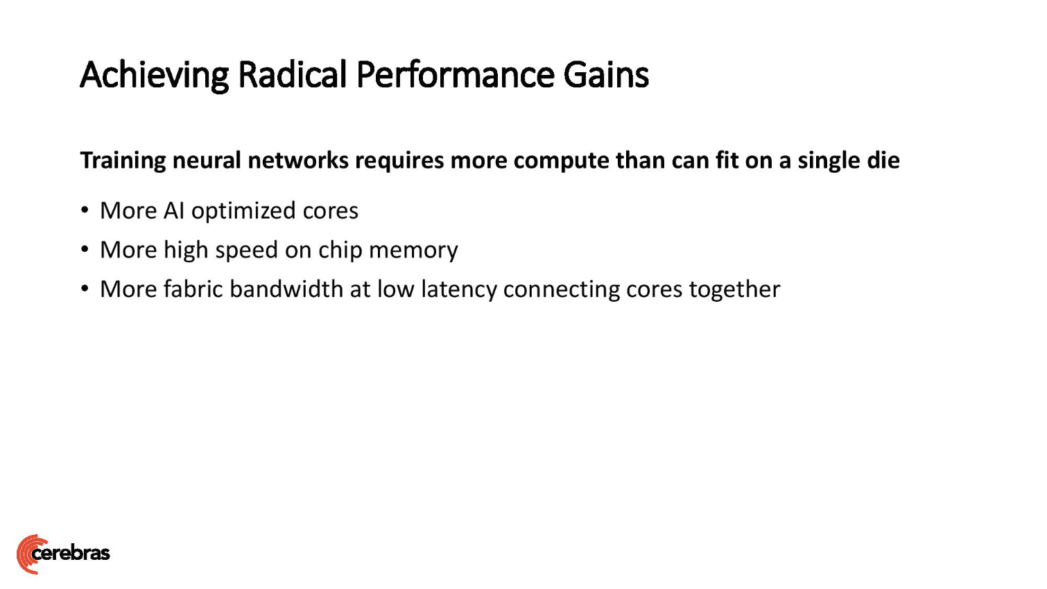
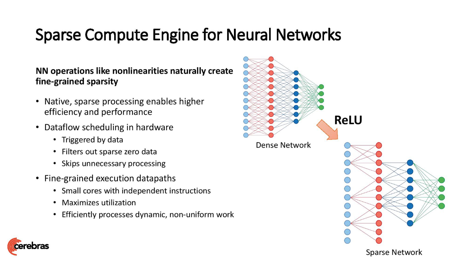
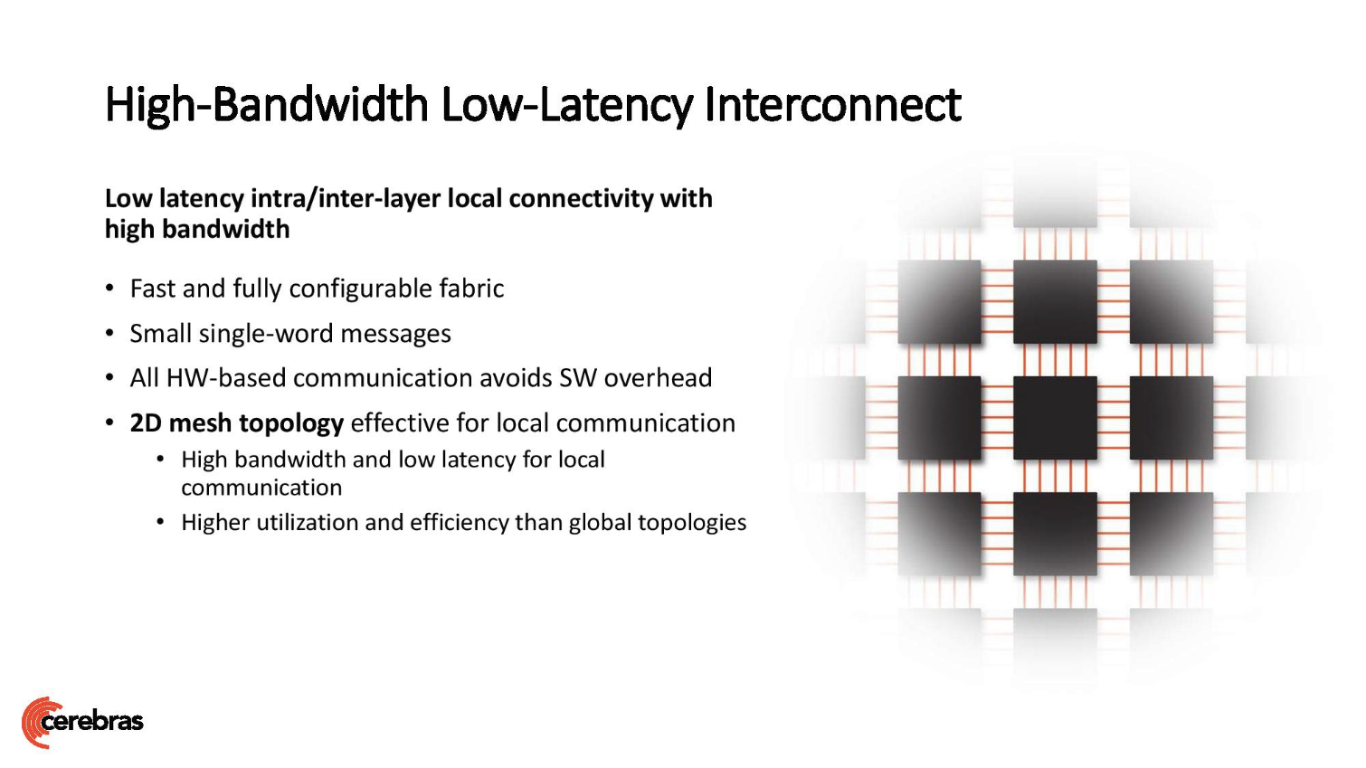
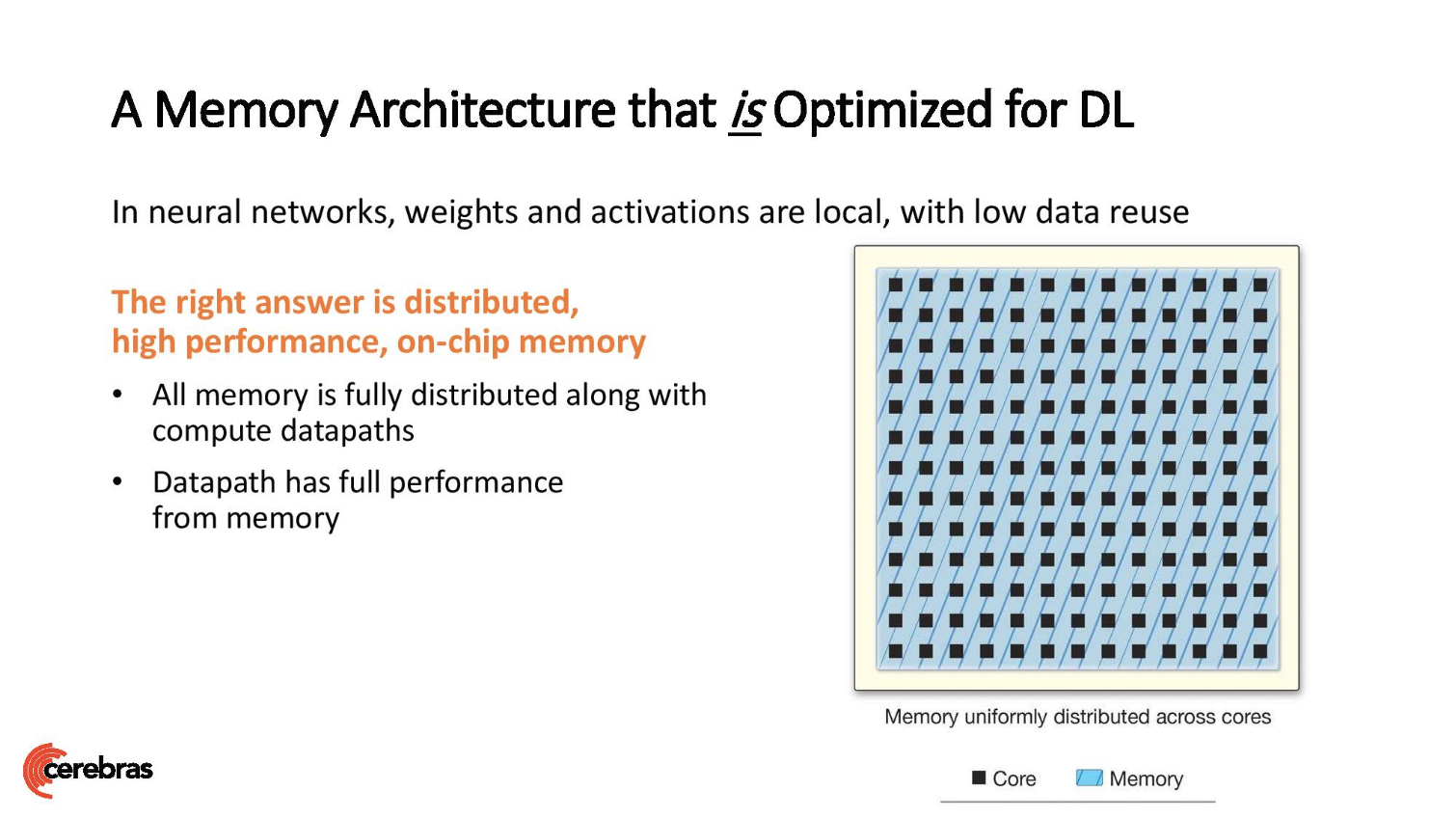
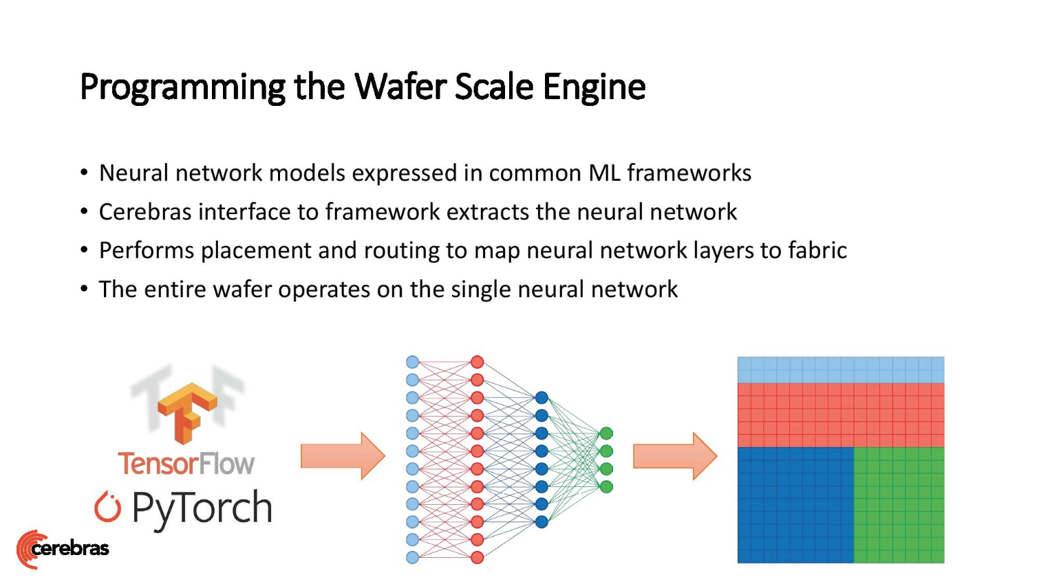
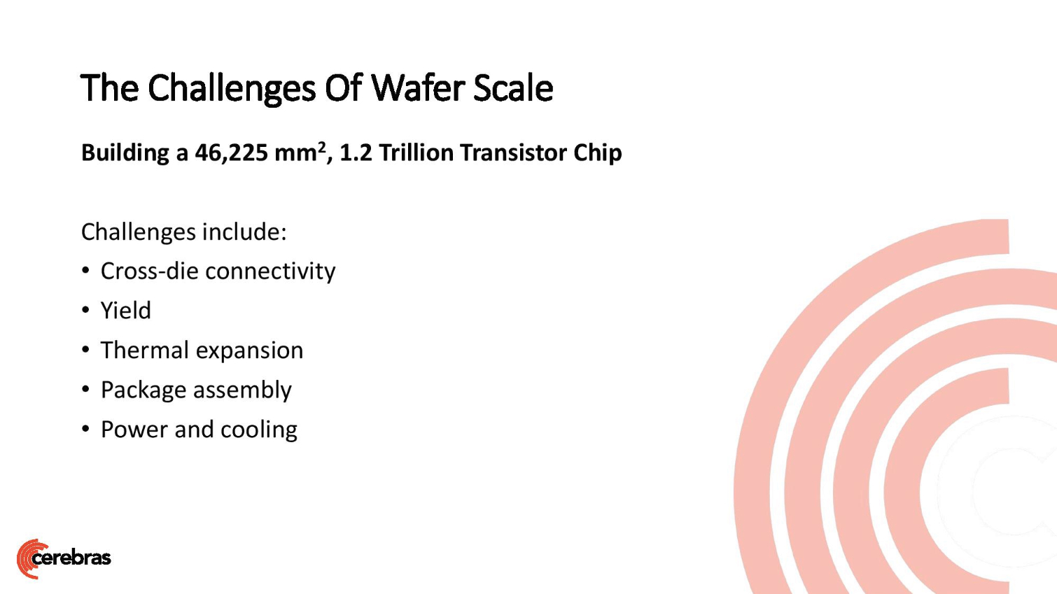
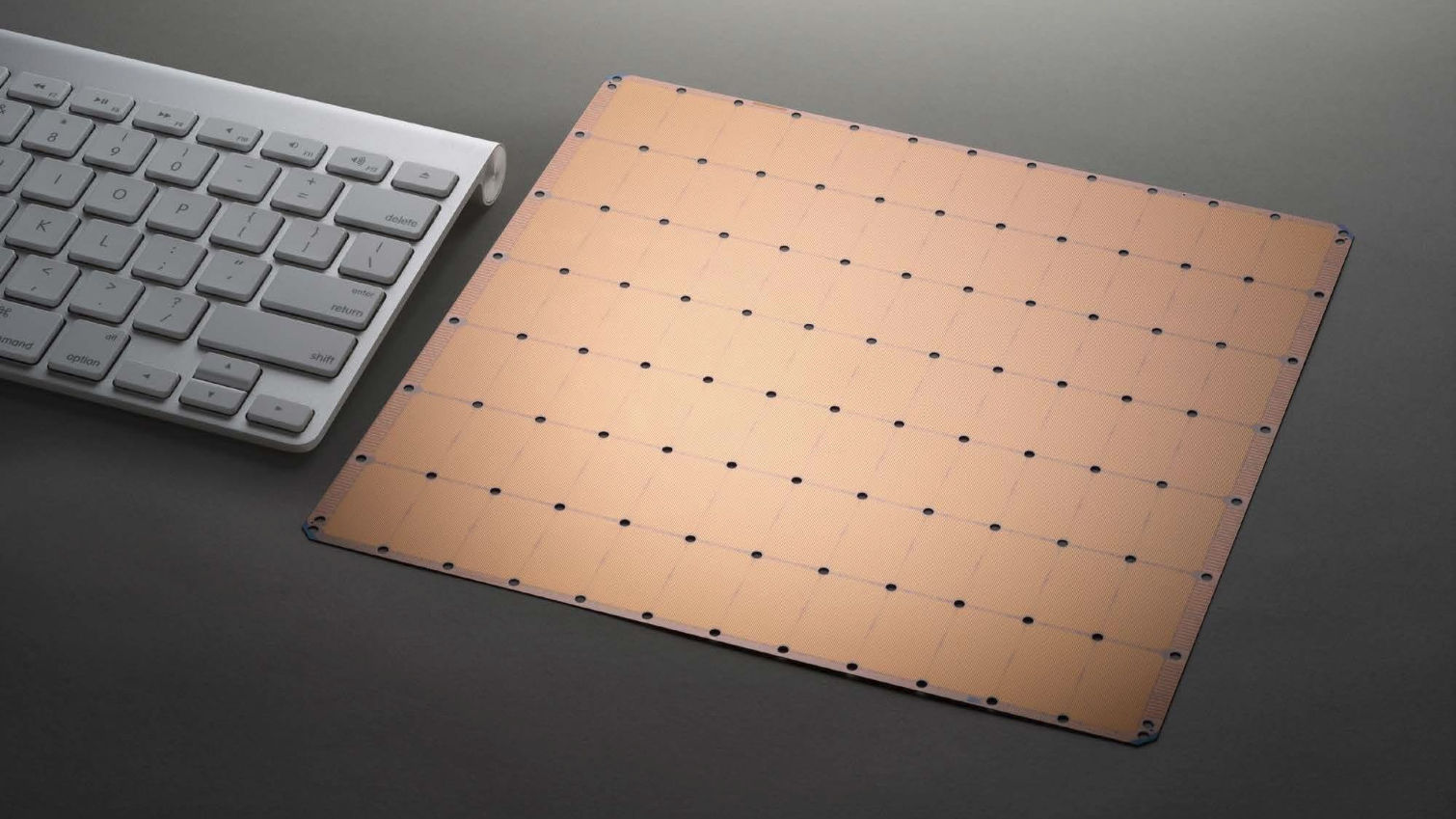
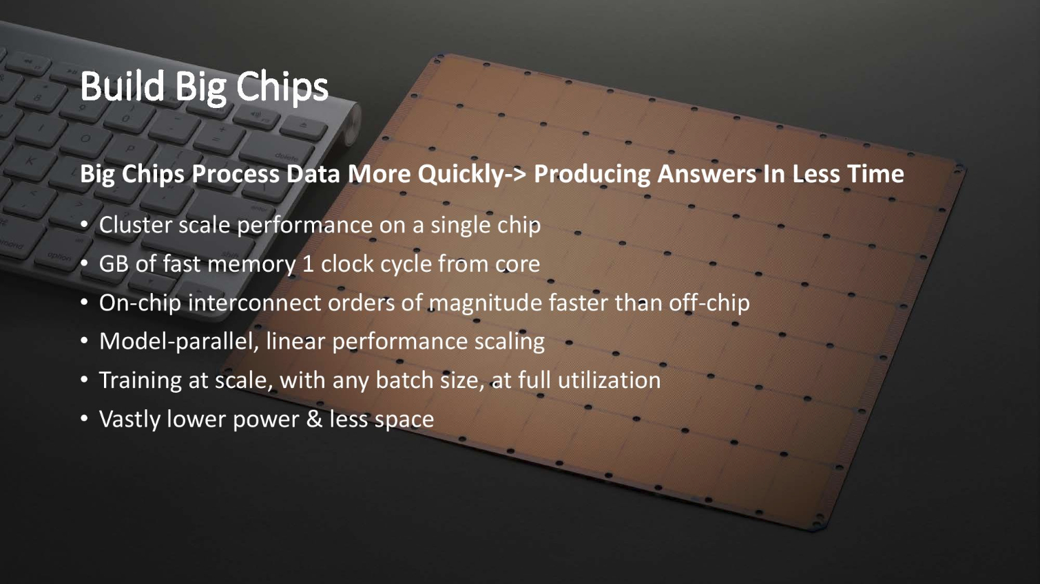
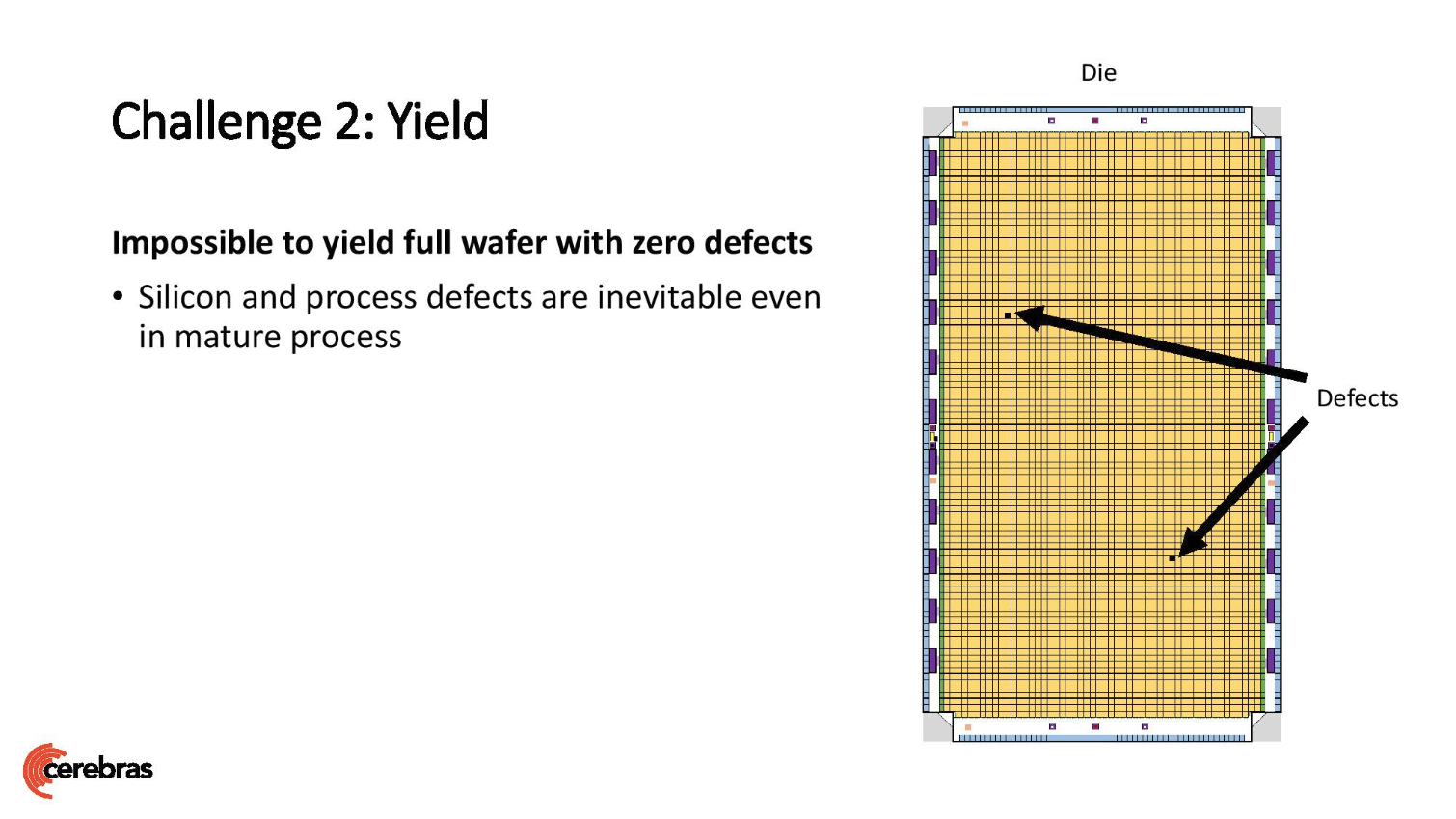
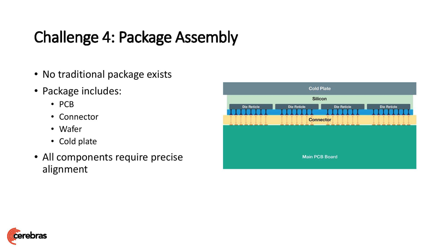
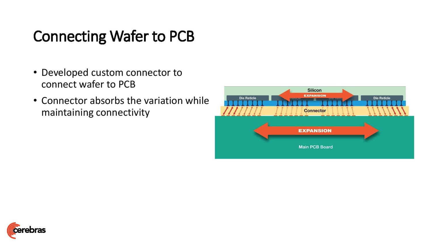


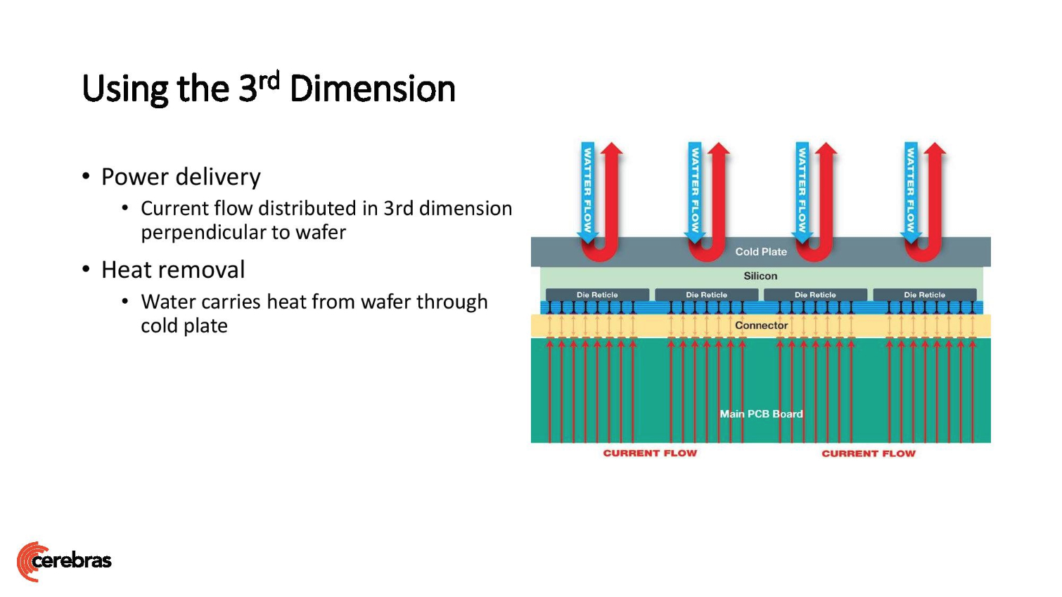
The Cerebras WSE's will find a home in the Argonne and Livermore National Laboratories, where they will be used in conjunction with existing supercomputers to speed AI-specific workloads.
The DOE's buy-in on the project is incredibly important for Cerebras, as it signifies that the chips are ready for actual use in production systems. Also, as we've seen time and again, trends in the supercomputing space often filter down to more mainstream usages, meaning further development could find Cerebras' WSE in more typical server implementations in the future.
The DOE also has a history of investing heavily in the critical software ecosystem needed for mass adoption, as we've seen with its investment in AMD's ROCM software suite for the exascale-class Frontier supercomputer, the work the agency is doing with Intel's OneAPI for the Aurora supercomputer, and the partnership with Cray for El Capitan.
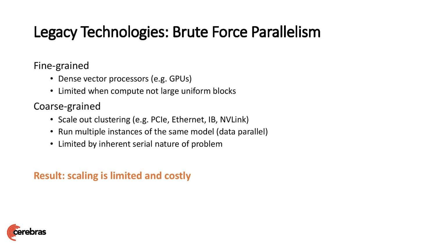
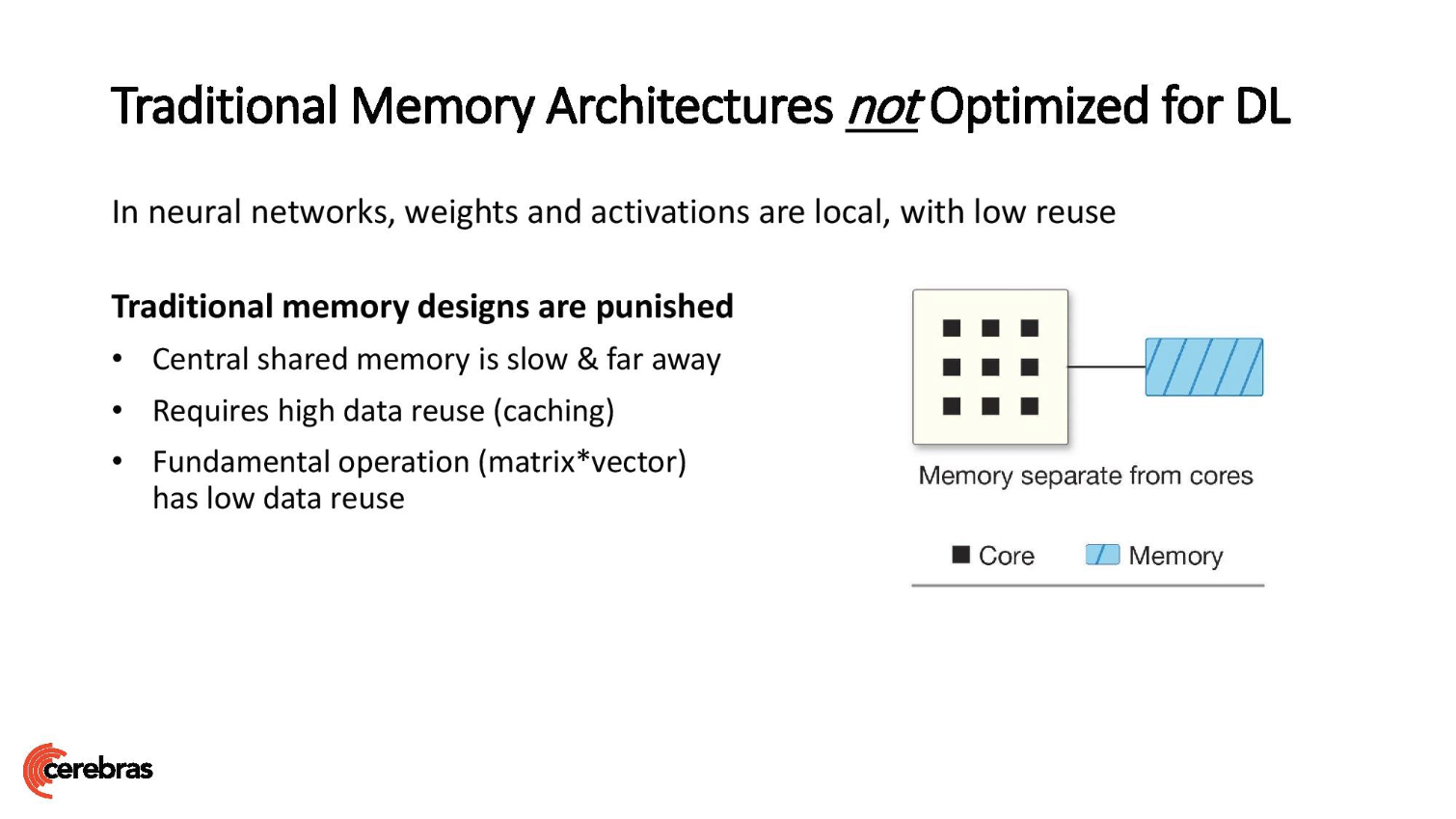
AI models are exploding in size as models double every five months. That doesn't currently appear to be a problem with the WSE's 18GB of SRAM memory, but because SRAM can't be scaled retroactively, larger models could soon outstrip the chips' native memory capacity. Cerebras tells us that it can simply use multiple chips in tandem to tackle larger workloads because, unlike GPUs, which simply mirror the memory across units (data parallel) when used in pairs (think SLI), the WSE runs in model parallel mode, which means it can utilize twice the memory capacity when deployed in pairs, thus scaling linearly. The company also says that scaling will continue with each additional wafer-size chip employed for AI workloads.
Get Tom's Hardware's best news and in-depth reviews, straight to your inbox.









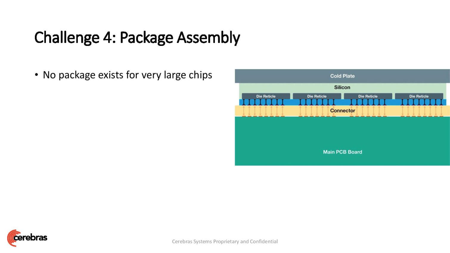

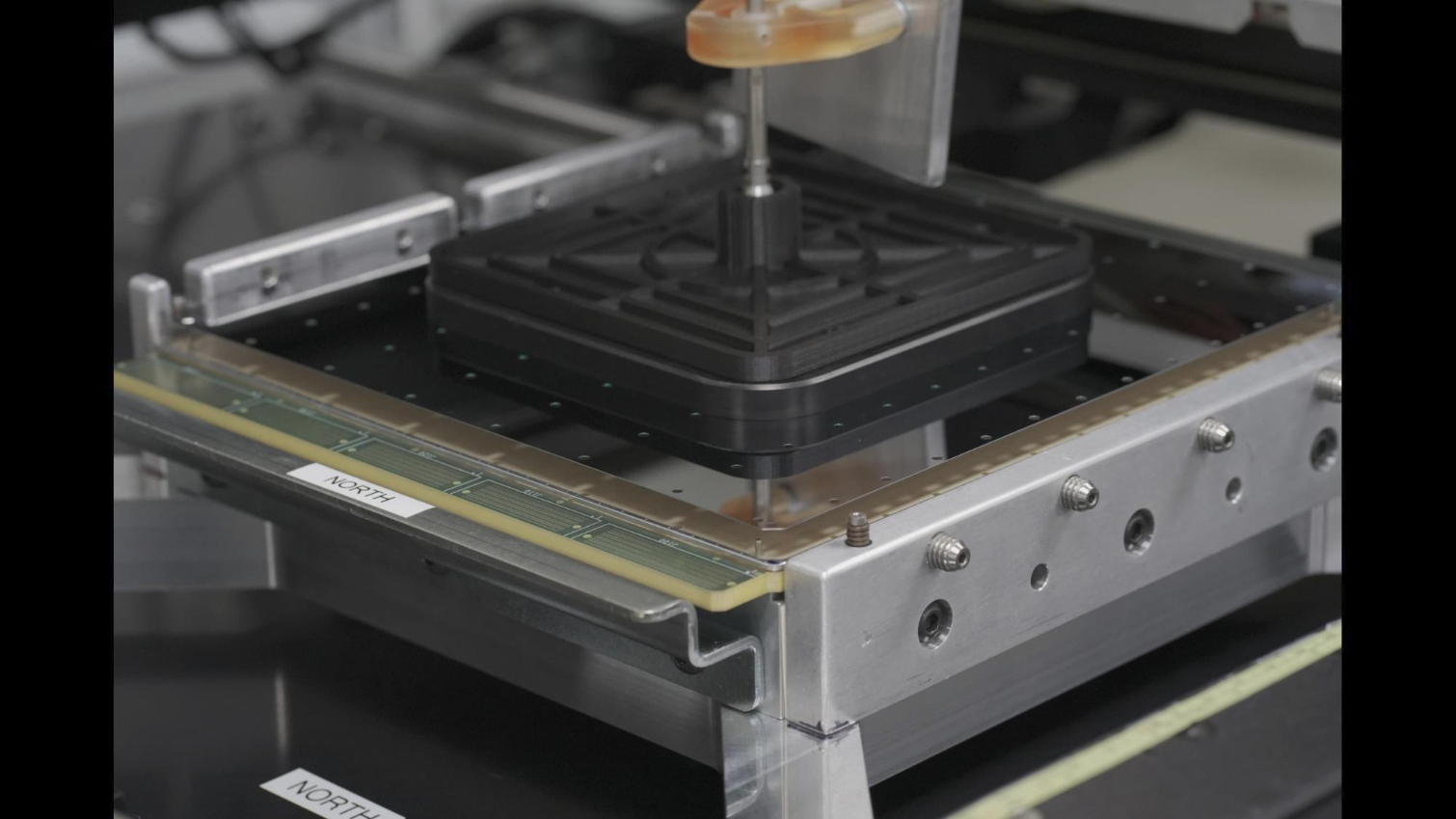

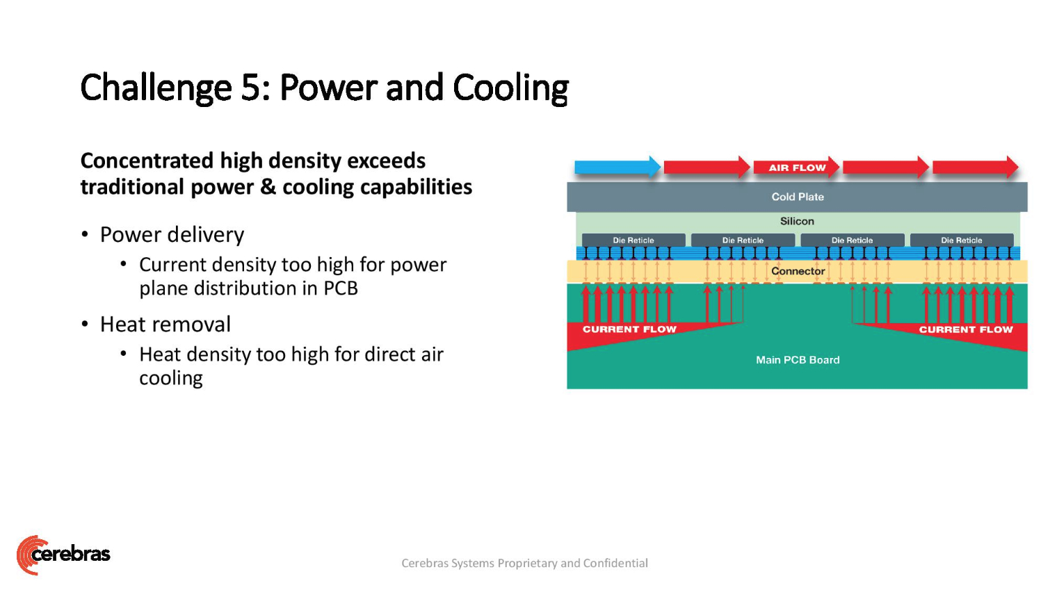
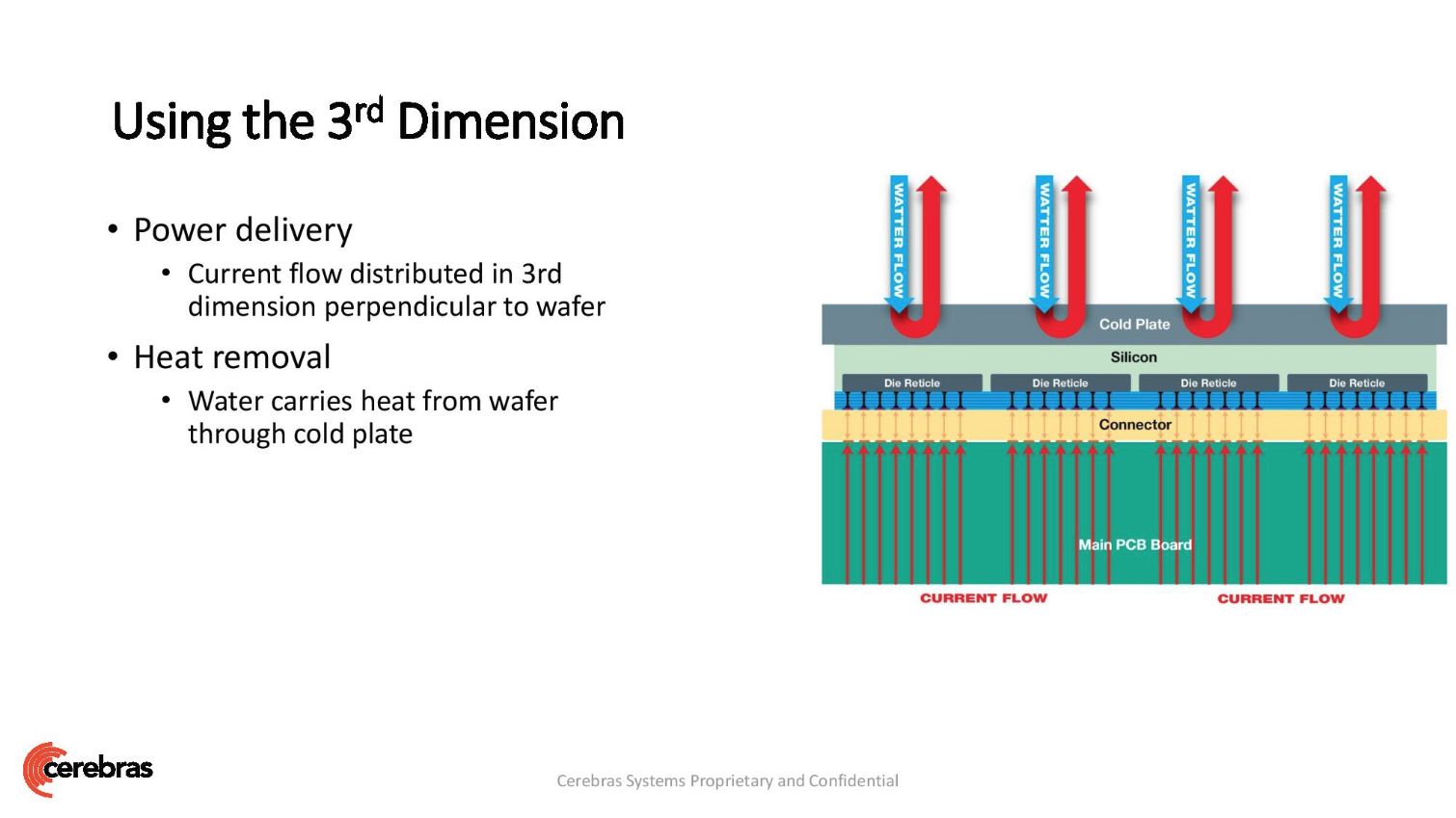
We're told that today's announcement just covers the basics of the partnership, but that more details, specifically in regards to co-development, will be shared at the Supercomputer tradeshow in November.

Paul Alcorn is the Editor-in-Chief for Tom's Hardware US. He also writes news and reviews on CPUs, storage, and enterprise hardware.
-
bit_user ReplyThe DOE's buy-in on the project is incredibly important for Cerebras, as it signifies that the chips are ready for actual use in production systems.
Um, I think the DoE invests in a lot of experimental tech. I wouldn't assume it necessarily means the tech is yet ready for end users.
Also, as we've seen time and again, trends in the supercomputing space often filter down to more mainstream usages, meaning further development could find Cerebras' WSE in more typical server implementations in the future.
Also, we've seen plenty of supercomputing tech that didn't filter down, like clustering, Infiniband, silicon-germanium semiconductors, and other stuff that I honestly don't know much about, because it hasn't filtered down. In fact, the story of the past few decades has been largely about the way that so much tech has filtered up from desktop PCs into HPC.
That's not tot say nothing filtered down - it's gone both ways. But the supercomputing industry used to be exclusively built from exotic, custom tech and has been transformed by the use of PCs, GPUs, and a lot of other commodity technology (SSDs, PCIe, etc.). Interestingly, it seems to be headed back in the direction of specialization, as it reaches scales and levels of workload-customization (such as AI) that make no sense for desktop PCs. I'd say this accelerator is a good example of that trend.
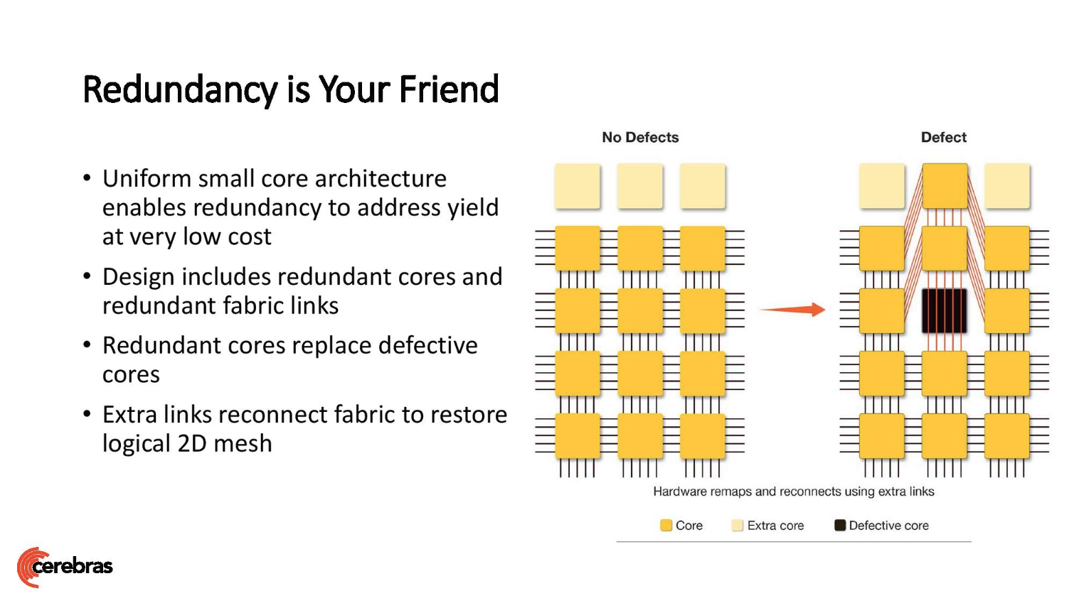
In particular, the problem with wafer-scale is that it will always be extremely expensive, because die space costs a certain amount per area. The better your fault-tolerance is, the less sensitive you are to yield, but it's still the case that die area costs a lot of money, as does their exotic packaging.
Cerebras tells us that it can simply use multiple chips in tandem to tackle larger workloads because, unlike GPUs, which simply mirror the memory across units (data parallel) when used in pairs (think SLI), the WSE runs in model parallel mode, which means it can utilize twice the memory capacity when deployed in pairs, thus scaling linearly.
This is silly. Of course you can scale models on GPUs in exactly the same way they're talking about.
Cool tech - and fun to read about, no doubt - but, this is exactly the sort of exotic tech that will remain the preserve of extreme high-end, high-budget computing installations. -
bit_user Reply
Apart from the cost issues I mentioned above, graphics has different data access patterns than AI. That's a big part of their pitch.InvalidError said:Now imagine a wafer-scale GPU!
Graphics needs fast random-access and is somewhat difficult to partition (unless you simply replicate the data, which makes the architecture less efficient in terms of power, performance, and cost). -
InvalidError Reply
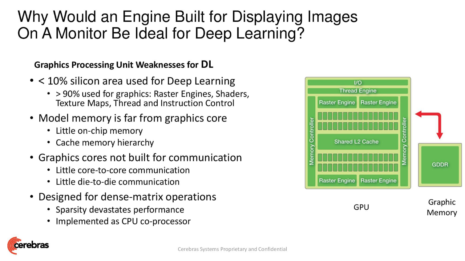
It is only "part of the pitch" because Cerebras uses SRAM, works particularly well for AI because each node in the neural network has a finite amount of data to keep track of. For a wafer-scale GPU which requires far more data accessibility and bandwidth multiplication, it would make sense to stack it with wafer-scale HBM.bit_user said:Apart from the cost issues I mentioned above, graphics has different data access patterns than AI. That's a big part of their pitch.
Having the option of duplicating data between channel is exactly why GPUs have multiple channels, nothing new there, sacrificing spatial efficiency for increased bandwidth and concurrency via duplication. It is also part of the reason why a given game uses an increasingly large amount of VRAM the more VRAM you have., more free space to duplicate stuff in, may as well use it to help balance load across memory channels and reduce average memory controller queue depth.bit_user said:Graphics needs fast random-access and is somewhat difficult to partition (unless you simply replicate the data, which makes the architecture less efficient in terms of power, performance, and cost). -
bit_user Reply
Whether it's SRAM or HBM, you're still talking about a distributed-memory GPU. If we've seen an example of that, especially with a mesh interconnect, I must've missed it. Feel free to enlighten me.InvalidError said:For a wafer-scale GPU which requires far more data accessibility and bandwidth multiplication, it would make sense to stack it with wafer-scale HBM.
The reason GPUs look the way they do (i.e. having cache hierarchies and big crossbars or otherwise massive internal buses) is that global memory is accessed pretty randomly.
That's an interesting theory. I've not encountered any support for that, in OpenGL, but I'm not familiar with Direct3D or Vulkan. So, if you have some good evidence of this, I'd be genuinely curious to see it.InvalidError said:Having the option of duplicating data between channel is exactly why GPUs have multiple channels, nothing new there, sacrificing spatial efficiency for increased bandwidth and concurrency via duplication. It is also part of the reason why a given game uses an increasingly large amount of VRAM the more VRAM you have., more free space to duplicate stuff in, may as well use it to help balance load across memory channels and reduce average memory controller queue depth.
Not that I can't believe it, but I've never actually heard of that practice. Furthermore, GPU memory topologies are something I find rather intriguing, because they're critical to efficiency and scalability. So, I've paid some attention to what has been disclosed about different GPUs - and it's not been much. That's not to say big game developers don't get a lot more info under NDA, but it's definitely not a detail that the GPU designers are publicizing in a way that would be required for most software to exploit.
AMD is pretty open about the details of their GPUs, not least because their Linux driver stack is almost entirely open source. Here's the RDNA architecture whitepaper - the most they say about the GDDR6 memory topology is that the memory controllers each have their own L2 slices and are 64-bit. The L2 cache lines are 128 bytes, but it's not clear whether or how the GDDR6 banks are interleaved - knowledge that would be critical for duplicating & load-balancing resources as you suggest.
https://www.amd.com/system/files/documents/rdna-whitepaper.pdf
Moreover, here's a D3D (DX12) memory allocator library they made, and nowhere do I see anything about replication or duplication:
https://gpuopen.com/gaming-product/d3d12-memory-allocator/https://github.com/GPUOpen-LibrariesAndSDKs/D3D12MemoryAllocator/blob/master/src/D3D12MemAlloc.h
Here's a whitepaper which discusses RDNA performance optimizations in depth, with quite a bit of time spent on memory. Except, it's all focused on LDS (Local Data Share - on chip memory local to each Workgroup Processor) and caches.
https://gpuopen.com/wp-content/uploads/2019/08/RDNA_Architecture_public.pdf
Also, note that they do make mention of a "Scalable Data Fabric", in both GCN (Vega) and RDNA (RX 5700). That contradicts the idea of distributed memory, as then you'd more likely be talking about a scalable compute fabric, with somewhat localized memory. -
InvalidError Reply
What is an interesting theory? Memory (read) bandwidth amplification? I hope not since there are countless examples of that starting with the venerable book, dead tree edition - the more copies you have, the more people can concurrently read it regardless of distance from the original source.bit_user said:That's an interesting theory. I've not encountered any support for that, in OpenGL, but I'm not familiar with Direct3D or Vulkan.
You won't find support for this in any API, it is a driver optimization thing: drivers know how much free VRAM there is and its location since they are in charge of managing VRAM and scheduling shaders, drivers detect that a memory channel consistently has a longer queue than others, duplicates some high-read-traffic assets (only reads can easily be amplified, which is fine since assets are generally static and drivers can manage memory coherency whenever an API call wants to modify them) in spare VRAM on whatever channels have the shortest queues and point some proportion of shaders to those duplicates to alleviate the bottleneck. If software requests more VRAM, drivers can pick which duplicates to scrap to most effectively service the new allocation request and existing workloads. There is no reason for the API to be aware of how drivers manage "unused VRAM", especially when you consider that drivers have to manage VRAM on a system-wide basis. I'd expect applications being able to force copies would be between sub-optimal and highly detrimental in most cases since forced copies would leave the GPU with less malleable VRAM to work with and increase its reliance on system RAM (much worse than sub-optimal VRAM memory queue depth) for overflows.
In an age where AMD, Nvidia and Intel are leapfrogging each other just about every meaningful generation with fancier texture compression techniques to get more mileage out of available memory bandwidth, using spare VRAM for bandwidth amplification is a wild strawberry - an ankle-high-hanging fruit.
This is similar to Windows using spare RAM for file system caching: software is generally unaware that the file system cache exists and the file system cache still counts as "free" as far as usual free memory reporting is concerned. The memory is being used but there is no reason for you to know about it since it can be freed whenever needed. -
bit_user Reply
I don't like to repeat myself, but I'll do so with emphasis: "if you have some good evidence of this, I'd be genuinely curious to see it. "InvalidError said:What is an interesting theory?
There are GPU performance analyzer tools that I'd imagine should be able to reveal this, if it's actually happening. So no "driver conspiracy theories" or flights of fancy, please.
I sometimes run into a D3D driver engineer for one of the Big Three GPU makers. I'll ask him about it and see if he'll tell me anything. -
InvalidError Reply
He should be able to at least tell you that user-land texture pixels are often represented in VRAM more than once for performance enhancement purposes.bit_user said:I sometimes run into a D3D driver engineer for one of the Big Three GPU makers. I'll ask him about it and see if he'll tell me anything. -
bit_user Reply
Okay, so I take it you've got nothing more than pure speculation. Thanks for being so forthright; such an exemplar.InvalidError said:He should be able to at least tell you that user-land texture pixels are often represented in VRAM more than once for performance enhancement purposes.
The main reason I participate in these forums is to exchange knowledge. I learn things and try to help educate others by sharing what I learn. Sometimes, things get petty, but that's my aspiration. Perhaps this sheds some insight into why I'm so bothered when people dissemble, spread misinformation, or misrepresent speculation as established fact - because it directly undermines both of my goals. I hope you can appreciate that perspective.
Anyway, I don't see him regularly, don't know him terribly well, and I don't know how much he'll tell me... but I'll ask. -
InvalidError Reply
It is the only way that a wafer-scale GPU could work.bit_user said:Okay, so I take it you've got nothing more than pure speculation.
It is also fundamentally what SLI/CF do: copy assets to all GPUs then split the workload between them.
A wafer-scale GPU could do the same thing, just far more efficiently thanks to having much faster links and tighter integration between GPUs.
