The History Of AMD CPUs
AMD K6-II+ And K6-III+
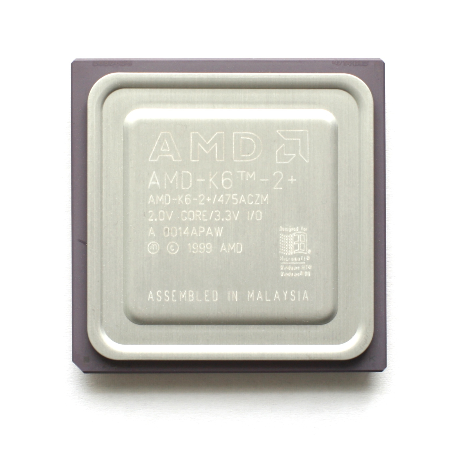
The last processors released by AMD in the K6 product line were the K6-II+ and K6-III+, which were targeted at the mobile market. These processors were similar to the K6-III in that they incorporated on-die L2 cache. The K6-II+ had 128 KB of L2, whereas the K6-III+ had 256 KB. Thanks to the use of AMD's 180 nm fab technology, these processors were relatively energy efficient.
AMD K6-II+ And K6-III+
| Code Name | N/A |
|---|---|
| Date | 2000 |
| Architecture | 32-bit |
| Data Bus | 32-bit |
| Address Bus | 32-bit |
| Maximum Memory Support | 4 GB |
| L1 Cache | 32 KB + 32 KB |
| L2 Cache | 128 - 256 KB (400 - 550 MHz) |
| L3 Cache | None |
| Clock Speed | 400 - 550 MHz |
| FSB | 100 MHz |
| SIMD | MMX, 3DNow! |
| Fab | 180 nm |
| Transistor Count | N/A |
| Power Consumption | N/A |
| Voltage | 1.6 - 2.0 V |
| Die Area | N/A |
| Socket | N/A |
AMD K7 And K75: The Birth Of Athlon
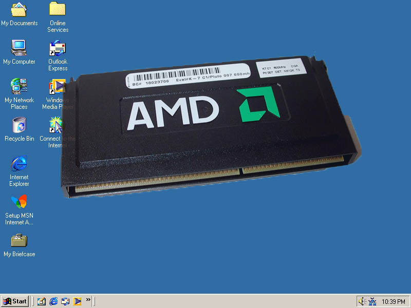
In 1999, AMD released its seventh-generation processor, the Athlon. It used a new architecture that increased IPC considerably and allowed AMD to push the clock rates up to 1 GHz. The FPU inside of AMD's previous processors had lagged behind competing Intel products, so improving the FPU was one of the primary objectives of the design team. This lead to the Athlon being equipped with an exceedingly powerful triple-issue out-of-order FPU that surpassed Intel's competing processors.
The first processor models placed the CPU core on a large silicon card. Instead of using on-die L2 cache, AMD used separate RAM chips soldered onto the same package as the CPU. This enabled AMD to install larger amounts of L2, but the cache ran at lower clock speeds.
Article continues belowLicensing DEC's EV6 FSB technology allowed AMD to design its own chipsets, leading to the first all-AMD platforms. Unfortunately, those first motherboards fell short of what Intel's competing 440BX could do. The EV6 FSB also made the Athlon compatible with new DDR RAM, which featured greater bandwidth and performance compared to traditional SDRAM.
AMD K7 And K75
| Code Name | Argon (K7) | Pluto, Orion (K75) |
|---|---|---|
| Date | June 1999 | November 1999 |
| Architecture | 32-bit | 32-bit |
| Data Bus | 32-bit | 32-bit |
| Address Bus | 32-bit | 32-bit |
| Maximum Memory Support | 4 GB | 4 GB |
| L1 Cache | 64 KB + 64 KB | 64 KB + 64 KB |
| L2 Cache | 512 KB (1/2 CPU) | 512 KB (1/2, 2/5, 1/3 CPU) |
| Clock Speed | 500 - 700 MHz | 550 - 850 MHz (Pluto)900 - 1000 MHz (Orion) |
| FSB | 100 MHz (DDR) | 100 MHz (DDR) |
| SIMD | MMX, Enhanced 3DNow! | MMX, Enhanced 3DNow! |
| Fab | 250 nm | 180 nm |
| Transistor Count | 22 Million | 22 Million |
| Power Consumption | 42 - 50 W | 31 - 65 W |
| Voltage | 1.6 V | 1.6 - 1.8 V |
| Die Area | 184 mm² | 102 mm² |
| Socket | Slot A | Slot A |
AMD K7: Athlon Thunderbird
Not long after the release of AMD's Athlon on Slot A and Intel's Pentium II and III for Slot 1, the industry realized that the lackluster performance of the L2 cache was hampering CPU performance. To overcome this issue, AMD reverted back to a traditional processor package with its Athlon Thunderbird, which contained L2 cache integrated directly onto the CPU die. Although the L2 cache size was cut in half, it ran at the same speed as the CPU, drastically improving performance.
Thanks to a maturing 180 nm process and higher yields, AMD also took this opportunity to boost the clock speed of its CPUs by 400 MHz.
AMD Athlon Thunderbird
| Code Name | Thunderbird |
|---|---|
| Date | 2000 |
| Architecture | 32-bit |
| Data Bus | 32-bit |
| Address Bus | 32-bit |
| Maximum Memory Support | 4 GB |
| L1 Cache | 64 KB + 64 KB |
| L2 Cache | 256 KB (Full Speed) |
| Frequency | 600 - 1400 MHz |
| FSB | 100, 133 MHz (DDR) |
| SIMD | MMX, Enhanced 3DNow! |
| Fab | 180 nm |
| Transistor Count | 37 Million |
| Power Consumption | 38 - 72 W |
| Voltage | 1.7 - 1.75 V |
| Die Area | 120 mm² |
| Socket | Socket A |
K7: AMD Duron
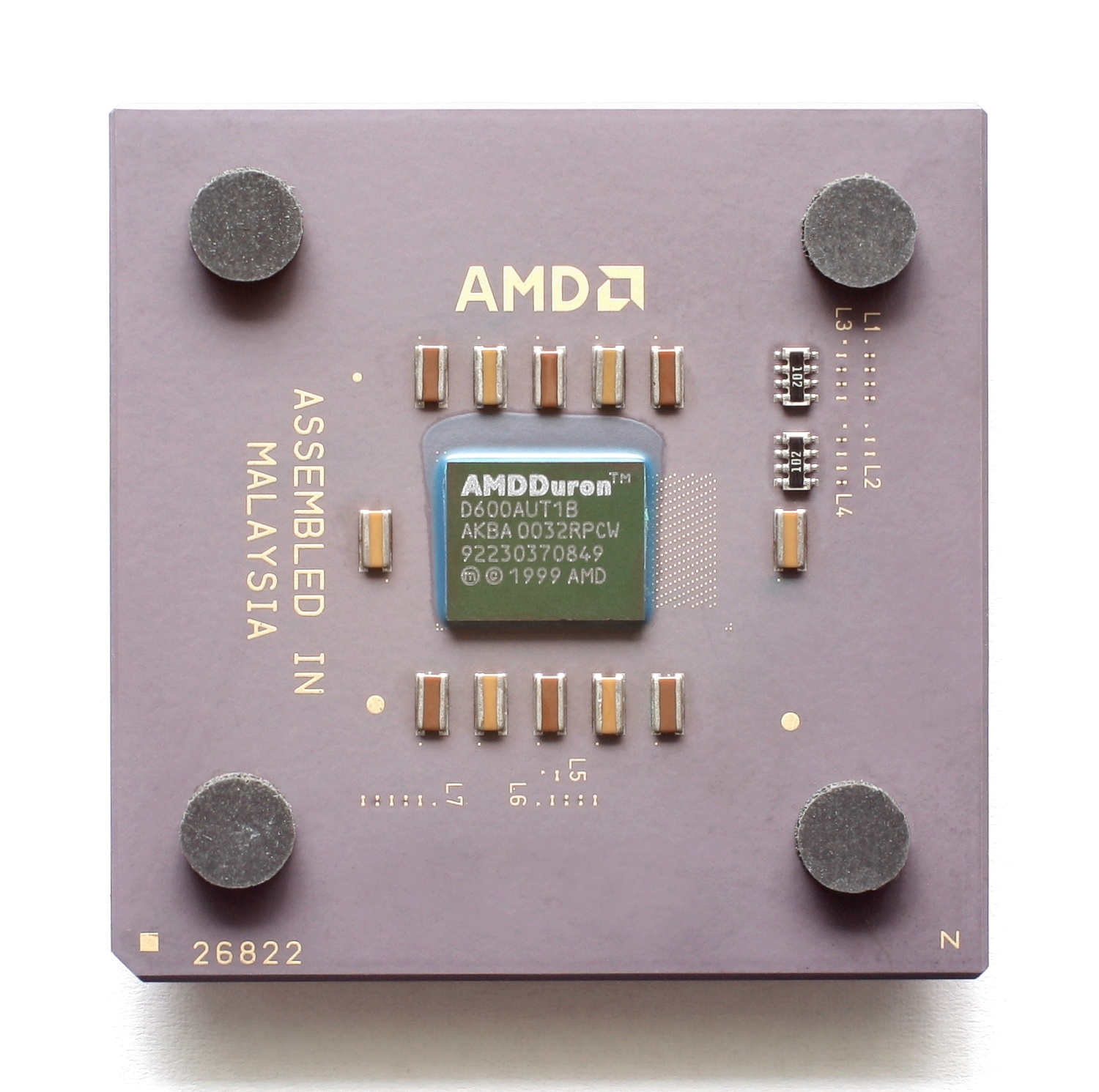
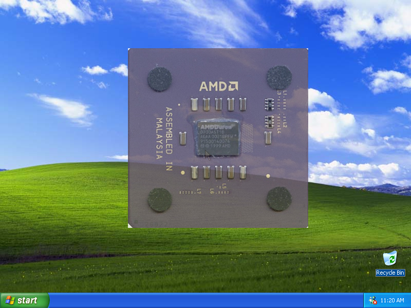
To target the entry-level segment and to make use of its lower yield chips, AMD introduced the Duron product line. These processors used the same architecture but generally ran at lower clock speeds. AMD also disabled all but 64 KB of the L2 cache on these processors, which reduced performance, but the Duron still was quite competitive against Intel's Celeron products.
Get Tom's Hardware's best news and in-depth reviews, straight to your inbox.
AMD Duron
| Code Name | Spitfire/Morgan |
|---|---|
| Date | 2000/2001 |
| Architecture | 32-bit |
| Data Bus | 32-bit |
| Address Bus | 32-bit |
| Maximum Memory Support | 4 GB |
| L1 Cache | 64 KB + 64 KB |
| L2 Cache | 64 KB (Full Speed) |
| Frequency | 600 - 950 MHz (Spitfire) 900 - 1300 MHz (Morgan) |
| FSB | 100 (DDR) |
| SIMD | MMX, Enhanced 3DNow! |
| Fab | 180 nm |
| Transistor Count | 37 Million |
| Power Consumption | N/A |
| Voltage | 1.5 - 1.75 V |
| Die Area | 120 mm² |
| Socket | Socket A |
AMD K7: Athlon Palomino/XP
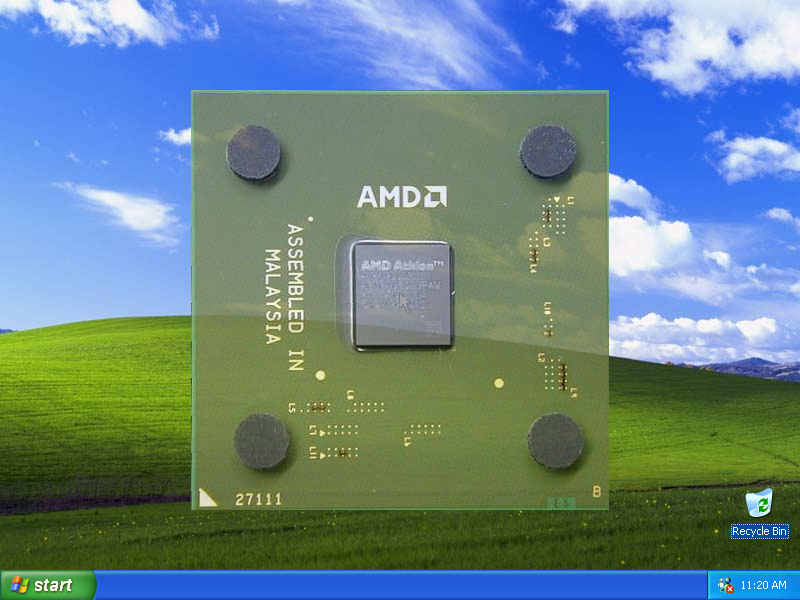
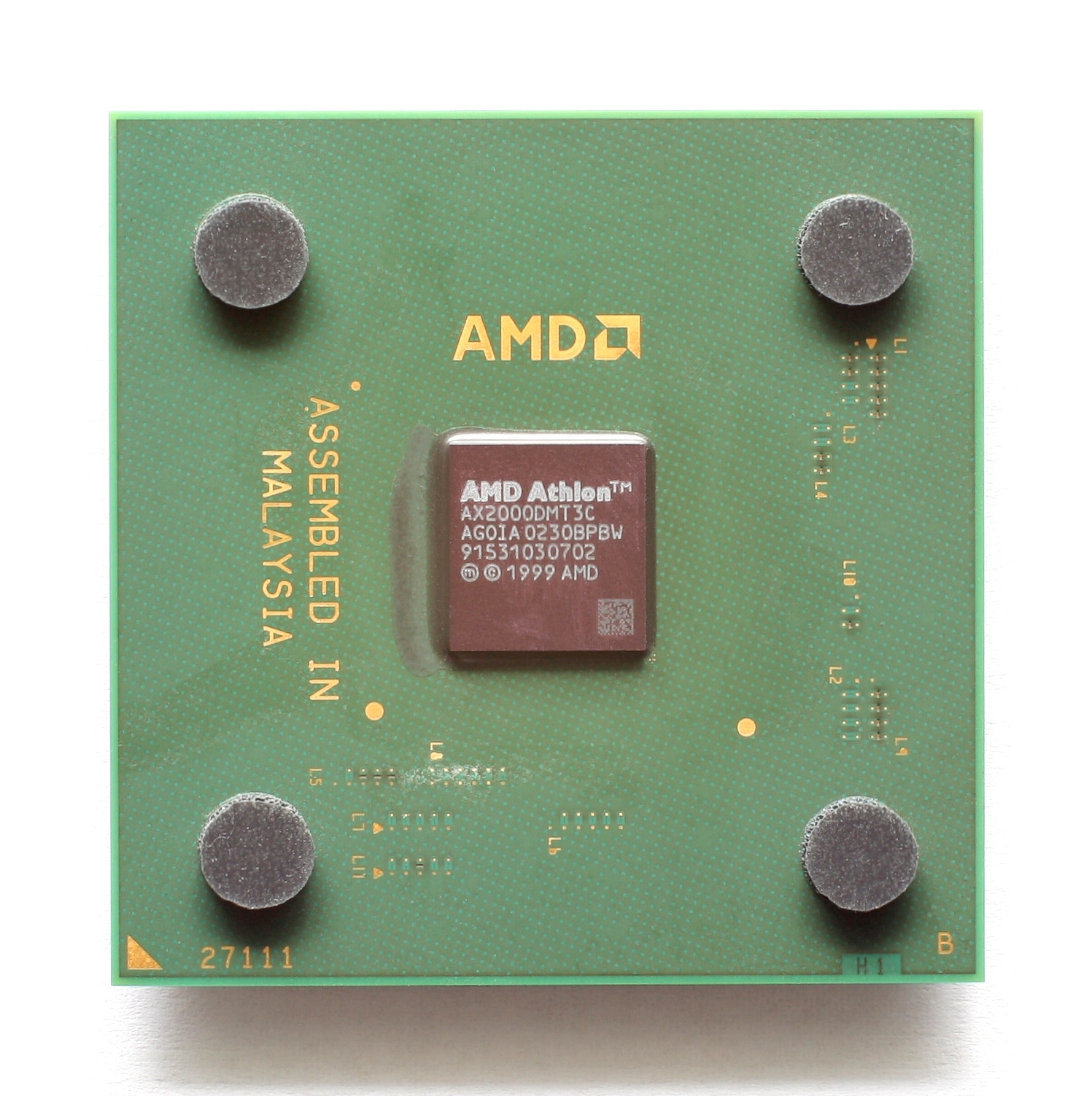
In 2001, AMD improved the Athlon again with the Palomino/XP. Little changed between the Thunderbird and the Palomino/XP, but the ever-maturing 180 nm process enabled AMD to push clock speeds up another 333 MHz. It also added support for the SSE SIMD instruction set. Microsoft's Windows XP launched around the same time, so AMD added "XP" to the Palomino code name to help advertise it towards users of the new operating system.
Versions of the Athlon Palomino/XP were also sold under the name "Athlon MP" for servers and "Athlon 4" or "Athlon XP Mobile" for laptop computers.
AMD Athlon Palomino/XP
| Code Name | Palomino/XP |
|---|---|
| Date | May 2001 |
| Architecture | 32-bit |
| Data Bus | 32-bit |
| Address Bus | 32-bit |
| Maximum Memory Support | 4 GB |
| L1 Cache | 64 KB + 64 KB |
| L2 Cache | 256 KB (Full Speed) |
| Frequency | 850 - 1733 MHz |
| FSB | 133 MHz (DDR) |
| SIMD | MMX, Enhanced 3DNow!, SSE |
| Fab | 180 nm |
| Transistor Count | 37.5 Million |
| Power Consumption | 46 - 72 W |
| Voltage | 1.75 V |
| Die Area | 129.26 mm² |
| Socket | Socket A |
AMD K7: Athlon Thoroughbred And Barton
In 2002, AMD rolled out the Athlon Thoroughbred, which was produced on a new 130nm process. This helped lower power consumption push frequencies over 2 GHz. As the process matured, AMD introduced the Barton a year later. Barton brought a modest clock rate increase, and it also doubled the size of the L2 cache and added support for 200 MHz FSB and 400 MHz DDR RAM.
AMD Athlon Thoroughbred and Barton
| Code Name | Thoroughbred | Barton |
|---|---|---|
| Date | April 2002 | February 2003 |
| Architecture | 32-bit | 32-bit |
| Data Bus | 32-bit | 32-bit |
| Address Bus | 32-bit | 32-bit |
| Maximum Memory Support | 4 GB | 4 GB |
| L1 Cache | 64 KB + 64 KB | 64 KB + 64 KB |
| L2 Cache | 256 KB (Full Speed) | 512 KB (Full Speed) |
| Frequency | 1 - 2.25 GHz | 1.3 - 2.33 GHz |
| FSB | 100 - 166 MHz (DDR) | 100 - 200 MHz (DDR) |
| SIMD | MMX, Enhanced 3DNow!, SSE | MMX, Enhanced 3DNow!, SSE |
| Fab | 130 nm | 130 nm |
| Transistor Count | 37.2 Million | 54.3 Million |
| Power Consumption | 49 - 68 W | 60 - 76 W |
| Voltage | 1.5 -1.65 V | 1.65 V |
| Die Area | 84.66 mm² | 100.99 mm² |
| Socket | Socket A | Socket A |
AMD K7: Athlon Thorton And Duron
Alongside Barton, AMD released two lower-end processors, the Athlon Thorton and a new Duron. Both processors used the same die as Barton but with part of the L2 cache disabled.
Thorton had 256 KB of L2 cache. similar to older Athlon processors, and it ran at slightly lower clock speeds than Barton. Thanks to the new 130nm fab technology, it was also more energy efficient than the older Athlon CPUs. The new Duron chip was limited to 64 KB of L2 cache, just like the previous Duron processors, but it was available at clock speeds up to 1.8 GHz, making the high-end models considerably faster than their predecessors.
AMD Athlon Thorton and Duron
| Code Name | Thorton | Duron |
|---|---|---|
| Date | 2003 | 2003 |
| Architecture | 32-bit | 32-bit |
| Data Bus | 32-bit | 32-bit |
| Address Bus | 32-bit | 32-bit |
| Maximum Memory Support | 4 GB | 4 GB |
| L1 Cache | 64 KB + 64 KB | 64 KB + 64 KB |
| L2 Cache | 256 KB (Full Speed) | 64 KB (Full Speed) |
| Frequency | 1.6 - 2.2 GHz | 1.4 - 1.8 GHz |
| FSB | 100 - 200 MHz (DDR) | 133 MHz (DDR) |
| SIMD | MMX, Enhanced 3DNow!, SSE | MMX, Enhanced 3DNow!, SSE |
| Fab | 130 nm | 130 nm |
| Transistor Count | 54.3 Million | 54.3 Million |
| Power Consumption | N/A | N/A |
| Voltage | 1.5 -1.65 V | 1.5 V |
| Die Area | 100.99 mm² | 100.99 mm² |
| Socket | Socket A | Socket A |
AMD Geode: The APU Predecessor
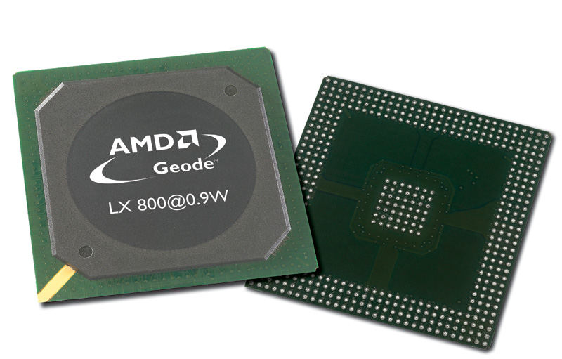
AMD purchased the Geode processor line in 2003 from National Semiconductor to extend its low-end product offerings. The Geodes actually had roots in another company called Cyrix, which created the MediaGX product line in the late 1990s as a single-chip solution containing a general-purpose processor, sound chip, graphics accelerator and all of the hardware typically inside of a motherboard's chipset. When Cyrix went out of business, National Semiconductor picked up the MediaGX and transformed it into the Geode.
AMD launched two processors under the "Geode" name. At the extreme low-end was the Geode GX series, which was identical to the products sold by National Semiconductor. As a somewhat higher-performance solution, AMD also introduced the LX series, which contained several enhancements including the transition to AMD's K7 Athlon architecture for the CPU. These products were highly efficient and were used in several inexpensive and thin-client devices.
AMD Geode
| Code Name | GX-Series | LX-Series |
|---|---|---|
| Date | 2003 | 2003 |
| Architecture | 32-bit | 32-bit |
| Data Bus | 32-bit | 32-bit |
| Address Bus | 32-bit | 32-bit |
| Maximum Memory Support | 4 GB | 4 GB |
| L1 Cache | 16 KB | 64 KB + 64 KB |
| L2 Cache | N/A | 128 KB (Full Speed) |
| Frequency | 333 - 400 MHz | 366 - 600 MHz |
| FSB | N/A | 166 - 200 MHz (DDR) |
| SIMD | N/A | N/A |
| Fab | N/A | 130 nm |
| Transistor Count | N/A | N/A |
| Power Consumption | N/A | N/A |
| Voltage | N/A | N/A |
| Die Area | N/A | N/A |
| Socket | N/A | N/A |
AMD K7: First Sempron
AMD released its first Sempron-branded products in 2004. Initially, they slid in between the high-end Athlon Barton processors and the low-end Duron, filling roughly the same space as the Athlon Thorton. The first few models used either Thorton or Thoroughbred cores with the full 256 KB of L2 cache. These chips were capped at slightly lower clock speeds, with the fastest SKUs clocked at 2 GHz.
Just a few months after Sempron was introduced, AMD released a new version based on the Barton core with the full 512 KB of L2 cache and a higher 2.2 GHz clock speed.
AMD Sempron
| Code Name | Thoroughbred/Thorton | Barton |
|---|---|---|
| Date | July 2004 | September 2004 |
| Architecture | 32-bit | 32-bit |
| Data Bus | 32-bit | 32-bit |
| Address Bus | 32-bit | 32-bit |
| Maximum Memory Support | 4 GB | 4 GB |
| L1 Cache | 64 KB + 64 KB | 64 KB + 64 KB |
| L2 Cache | 256 KB (Full Speed) | 512 KB (Full Speed) |
| Frequency | 1.5 - 2.0 GHz | 2 - 2.2 GHz |
| FSB | 166 MHz (DDR) | 166 - 200 MHz (DDR) |
| SIMD | MMX, Enhanced 3DNow!, SSE | MMX, Enhanced 3DNow!, SSE |
| Fab | 130 nm | 130 nm |
| Transistor Count | 37.2 - 54.3 Million | 54.3 Million |
| Power Consumption | N/A | N/A |
| Voltage | 1.6 V | 1.6 - 1.65 V |
| Die Area | 84.66 - 100.99 mm² | 100.99 mm² |
| Socket | Socket A | Socket A |
AMD K8: Athlon 64!
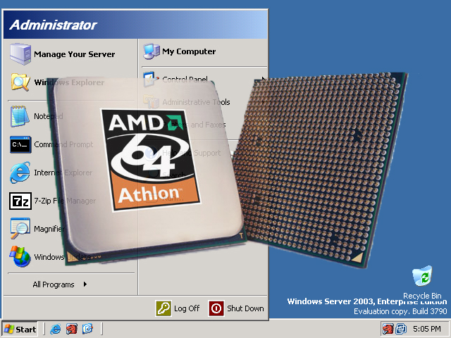
In 2003, AMD shocked the world by introducing the first consumer-oriented 64-bit x86 processor. Codenamed "K8," these processors were essentially heavily modified variations of the K7. By moving to a 64-bit design, AMD was able to extend the memory support to a theoretical 1 TB.
Although that was more RAM than any K8 system would ever use, PCs were no longer limited to 4 GB of memory, and systems with 8 GB of RAM began showing up on the market. AMD also moved the memory controller from its chipset and integrated it into the CPU die. This drastically reduced memory latency and pushed performance up considerably over the K7. With the memory controller inside of the CPU die, this effectively removed the FSB from the system. Instead, AMD introduced its HyperTransport technology, which was capable of significantly greater bandwidth than the older FSB connection.
AMD sold the initial batch of K8 chips under the brand names "Athlon 64" for consumers (Clawhammer and Newcastle), "Athlon 64 FX" (Sledgehammer and Clawhammer) for enthusiasts and "Opteron" for servers (Sledgehammer).
AMD Athlon 64 Sledgehammer, Clawhammer and Newcastle
| Code Name | Sledgehammer | Newcastle/Clawhammer |
|---|---|---|
| Date | 2003/2004 | 2004 |
| Architecture | 64-bit | 64-bit |
| Data Bus | 64-bit | 64-bit |
| Address Bus | 64-bit | 64-bit |
| Maximum Memory Support | 1 TB | 1 TB |
| L1 Cache | 64 KB + 64 KB | 64 KB + 64 KB |
| L2 Cache | 1 MB (Full Speed) | 512 KB (Full Speed - Newcastle), 1 MB (Full Speed - Clawhammer) |
| Clock Speed | 1.4 - 2.4 GHz | 1.8 - 2.4 GHz (Newcastle)/ 2 - 2.6 GHz (Clawhammer) |
| Memory Controller | Single-Channel 400 MHz DDR | Single-Channel 400 MHz DDR (Socket 754)/ Dual-Channel 400 MHz DDR (Socket 939) |
| HyperTransport | 800 MHz | 800-1000 MHz |
| SIMD | MMX, Enhanced 3DNow!, SSE, SSE2 | MMX, Enhanced 3DNow!, SSE, SSE2 |
| Fab | 130 nm | 130 nm |
| Transistor Count | 105.9 Million | 105.9 Million |
| Power Consumption | 89 W TDP | 89 W TDP |
| Voltage | 1.5 - 1.55 V | 1.5 V |
| Die Area | 193 mm² | 193 mm² |
| Socket | Socket 940 | Socket 754, Socket 939 |
-
wurkfur ReplyThe eternal underdog will once more have his day.
How can you say eternal? For a good while AMD was actually making faster and more innovative stuff than Intel.
AMD launched dual cores for consumers
AMD integrated memory controllers on die
AMD created x64 versus Intel pushing the move to a new architecture that only they could make
AMD also pushed APU's mainstream
Intel adopted all these practices after the fact while engaging in illegal monopolistic behavior in an international stage that stifled innovation, cost jobs, and caused consumers to pay more.
One could argue that if Intel had simply played by the rules locally and abroad, AMD would have had enough cash flow to maintain their position through better R&D instead of playing catch up.
For that very reason I look forward to AMD's upcoming products to replace my 1090t that's clocked within an inch of its life. -
vern72 ReplyAMD launched dual cores for consumers
AMD integrated memory controllers on die
AMD created x64 versus Intel pushing the move to a new architecture that only they could make
AMD also pushed APU's mainstream
And one more thing: AMD was the first to ship a 1Ghz x86 CPU to the masses. -
CaedenV Fantastic article! Especially loved seeing the early chips; I had no idea that they were in the game pre 286 generation. I was a kid at the time and my understanding was that the law suits at the time were what allowed AMD (and Via... don't forget the 'true underdog' lol) to ENTER the market, not remain in it.Reply
Also, I remember endless debates when I built my first PC for college ~2001. I wanted an AMD XP chip... but my video editing software had issues with it (some sort of audio processing bug. Then it was between the Pentium 4 which had great burst performance, but terrible sustained performance due to RDRAM that could not keep up; and the Pentium 3 which looked terrible on paper and was 'old', but had fantastic sustained performance (and much healthier thermals!). In the end I decided on the Pentium 3, but (noob build mistake) because I bought a crap PSU it died within a year and I moved to my one and only AMD build which was a 2GHz Barton. That was a great PC that lasted a solid 3 years.
I was really sad to watch Bulldozer fall apart. After the Core2Duo AMD was falling behind and bulldozer was supposed to bring them back into relevance. But then the marketing department thought that nobody would buy a high-end $500+ CPU, so they slashed the cache to make it more affordable. Sadly that cache was needed to prevent the CPU from constantly going back to the system memory for instructions and it literally killed the product. And Intel happily sold several $400-1000 i7 chips while AMD could not even hold onto the budget market. Sad times. It is a shame that they were not able to sell the full chip as originally designed, and then cut down a cheap version for 'consumers'.
But now it looks like AMD is starting to play ball again. Next 3 years will be interesting to watch, and if they make a winner then I might throw my hat in their ring again when I do a rebuild 2-4 years from now. I would love to see something blow my 4.2GHz Sandy Bridge out of the water! -
CaedenV ReplyOld CPUs are so much... cooler than new ones.
you kidding? Those old chips ran meltingly hot! And with tons of power! when those old chips were OC'd they could drink down nearly 200W and easily heat a dorm room on cold winter nights! -
turkey3_scratch Reply17879424 said:Old CPUs are so much... cooler than new ones.
you kidding? Those old chips ran meltingly hot! And with tons of power! when those old chips were OC'd they could drink down nearly 200W and easily heat a dorm room on cold winter nights!
To be fair we have current GPUs on the market above 300W.
But by "cool" I just meant "cool" as in "vintage". -
SinxarKnights It is amazing to think that my old 433Mhz Intel processor was pretty good at the time. With 256MB of RAM the OS (Win98SE) was very responsive. The motherboard didn't have an AGP slot so I had to settle for a Nvidia GeForce FX 5200 from Wal-mart. Still have lots of fond memories of Diablo and Ultima Online.Reply
I built a PC with an Athlon 64 X2 5600+. Due to the larger cache, it gave a significant performance increase over the other lower tiered CPUs. This was right at the time Intel came out with the Core architecture. While the top end 64 X2 series (6000+ and up) outperformed the first Core CPUs that were released, everything went downhill from there for AMD.
15 years ago my awesome 433mhz CPU was awesome, today it cannot perform the most basic of task in a timely manner. I imagine 15 years from now my current 4790k will be in the same boat. -
Zachary Singer-Englar I still brag about my Athlon II x250 Regor. That was a great processor for an underfunded enthusiast, It shipped at 3.0 and i had it clocked to 3.5 for about 2 years on a stock cooler before I replaced the whole set-up because my motherboard gave out (probably unrelated to my overclocking). That was 5 years after I had purchased the processor. My FX-6350 is not holding up quite as well.Reply
