The History Of AMD CPUs
AMD K8: Gradual Improvement
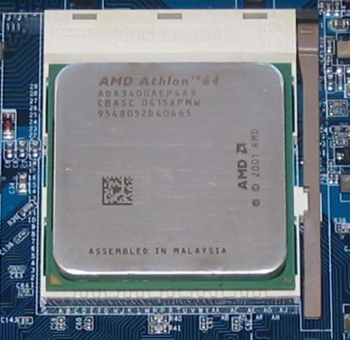
In 2004, AMD introduced its new 90nm transistor process, which enabled the company to increase the performance of its Athlon 64 processors while also reducing power consumption. AMD produced a total of four 90nm Athlon 64 chips to cover the desktop market.
Venice became the last Athlon 64 processor released for AMD's Socket 754, and it also was the highest-performing chip available on that platform. AMD's San Diego ran at similar clock speeds, but was targeted at the Socket 939 platform and had a larger 1 MB L2 cache.
To target more efficient systems, AMD introduced the Winchester core around the same time, which had a lower TDP of 67 W. It was the most energy efficient Athlon 64 processor for several years until the release of the 62 W TDP Orleans in 2006 and the 65nm 45 W Lima in 2007.
Article continues belowAMD Athlon 64 Winchester, Venice, San Diego, Orleans and Lima
| Code Name | Winchester/Venice/San Diego | Orleans/Lima |
|---|---|---|
| Date | 2004 (Winchester)/2005 (Venice and San Diego) | 2006 |
| Architecture | 64-bit | 64-bit |
| Data Bus | 64-bit | 64-bit |
| Address Bus | 64-bit | 64-bit |
| Maximum Memory Support | 1 TB | 1 TB |
| L1 Cache | 64 KB + 64 KB | 64 KB + 64 KB |
| L2 Cache | 512 KB (Full Speed - Winchester and Venice)/ 1 MB (Full Speed - San Diego) | 512 KB (Full Speed - Orleans and Lima), 1 MB (Full Speed - Lima) |
| Clock Speed | 1.8 - 2.2 GHz (Winchester)/ 1.8 - 2.4 GHz (Venice)/ 2.2 - 2.6 GHz (San Diego) | 1.8 - 2.6 GHz (Orleans)/ 2 - 2.8 GHz (Lima) |
| Memory Controller | Single-Channel 400 MHz DDR (Venice)/ Dual-Channel 400 MHz DDR (Winchester and San Diego) | Dual-Channel DDR2 |
| HyperTransport | 800 MHz (Venice)/ 1000 MHz (Winchester and San Diego) | 800-1000 MHz |
| SIMD | MMX, Enhanced 3DNow!, SSE, SSE2, SSE3 | MMX, Enhanced 3DNow!, SSE, SSE2, SSE3 |
| Fab | 90 nm | 90 nm (Orleans)/ 65 nm (Lima) |
| Transistor Count | N/A | N/A |
| Power Consumption | 64 W TDP (Winchester)/ 89 W TDP (Venice and San Diego) | 62 W (Orleans)/ 45 W (Lima) |
| Voltage | 1.35 - 1.4 V | 1.25 - 1.4 V |
| Die Area | N/A | N/A |
| Socket | Socket 754 (Venice)/ Socket 939 (Winchester and San Diego) | Socket AM2 |
AMD K8: Sempron
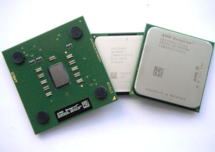
Alongside the K8 Athlon processors, AMD also updated its Sempron product line with the new K8 architecture. Just like the first Sempron products, these CPUs typically had less cache and lower clock speeds than their Athlon counterparts.
AMD K8 Sempron
| Code Name | Paris, Palermo, Manila, Sparta |
|---|---|
| Date | 2004 - 2007 |
| Architecture | 64-bit |
| Data Bus | 64-bit |
| Address Bus | 64-bit |
| Maximum Memory Support | 1 TB |
| L1 Cache | 64 KB + 64 KB |
| L2 Cache | 128 - 512 KB (Full Speed) |
| Clock Speed | 1.4 - 2.3 GHz |
| Memory Controller | Single-Channel DDR / Dual-Channel DDR / Dual-Channel DDR2 |
| HyperTransport | 800 MHz / 1000 MHz |
| SIMD | MMX, Enhanced 3DNow!, SSE, SSE2, SSE3 |
| Fab | 130 - 65 nm |
| Transistor Count | N/A |
| Power Consumption | N/A |
| Voltage | 1.2 - 1.4 V |
| Die Area | N/A |
| Socket | Socket 754 / Socket 939 / Socket AM2 |
AMD K8: Athlon 64 X2
Just as it did two years prior, AMD pulled another shocker in 2005 with the introduction of a consumer-oriented dual-core processor based on the K8 architecture. Although the two processors were incapable of working on the same thread simultaneously, the second CPU core could handle other tasks and increase multitasking performance.
AMD produced a total of six CPU configurations in the Athlon 64 X2 product line, but the first five are all relatively similar to each other, varying only in L2 cache size and clock rate. The sixth Athlon 64 X2 design was the fastest in the series and the most energy efficient, owing to the move to 65nm transistor technology.
AMD Athlon 64 X2
| Code Name | Manchester - Windsor | Brisbane |
|---|---|---|
| Date | 2005-2006 | 2006 |
| Architecture | 64-bit | 64-bit |
| Data Bus | 64-bit | 64-bit |
| Address Bus | 64-bit | 64-bit |
| Maximum Memory Support | 1 TB | 1 TB |
| L1 Cache | 64 KB + 64 KB Per Core | 64 KB + 64 KB Per Core |
| L2 Cache | 256 KB - 1 MB Per Core (Full Speed) | 512 KB Per Core (Full Speed) |
| Clock Speed | 2 - 3.2 GHz | 1.9 - 3.1 GHz |
| Memory Controller | Dual-Channel DDR/DDR2 | Dual-Channel DDR2 |
| HyperTransport | 1000 MHz | 1000 MHz |
| SIMD | MMX, Enhanced 3DNow!, SSE, SSE2, SSE3 | MMX, Enhanced 3DNow!, SSE, SSE2, SSE3 |
| Fab | 90 nm | 65 nm |
| Transistor Count | N/A | N/A |
| Power Consumption | 35 - 125 W TDP | 65 - 89 W TDP |
| Voltage | 1.25 - 1.4 V | 1.25 - 1.35 V |
| Die Area | N/A | 126 mm² |
| Socket | Socket 939, Socket AM2 | Socket AM2 |
AMD K8: Turion And Turion X2
AMD introduced a new mobile product line called "Turion" in 2005. These processors used the same architecture as AMD's desktop product, but thanks to careful core binning, they were able to operate with less power. AMD introduced dual-core variants as well, dubbed "Turion X2."
Get Tom's Hardware's best news and in-depth reviews, straight to your inbox.
AMD K8 Turion and Turion X2
| Code Name | Turion (Lancaster, Richmond, Sable) | Turion X2 |
|---|---|---|
| Date | 2005 - 2008 | 2006 - 2008 |
| Architecture | 64-bit | 64-bit |
| Data Bus | 64-bit | 64-bit |
| Address Bus | 64-bit | 64-bit |
| Maximum Memory Support | 1 TB | 1 TB |
| L1 Cache | 64 KB + 64 KB | 64 KB + 64 KB |
| L2 Cache | 512 KB - 1 MB (Full Speed) | 256 KB - 1 MB Per Core (Full Speed) |
| Clock Speed | 1.6 - 2.4 GHz | 1.6 - 2.5 GHz |
| Memory Controller | Single-Channel DDR / Dual-Channel DDR2 | Dual-Channel DDR2 |
| HyperTransport | 800 MHz / 1000 MHz | 800-1000 MHz |
| SIMD | MMX, Enhanced 3DNow!, SSE, SSE2, SSE3 | MMX, Enhanced 3DNow!, SSE, SSE2, SSE3 |
| Fab | 65 - 90 nm | 65 - 90 nm |
| Transistor Count | N/A | N/A |
| Power Consumption | 25 - 35 W | 31 - 35 W |
| Voltage | 0.8 - 1.35 V | N/A |
| Die Area | N/A | N/A |
| Socket | Socket 754 / Socket S1 | Socket S1 |
AMD K10: Quad-Core Phenom
AMD's next architecture, K10, was a rather ambitious design. It is closely related to the K8, but it had several enhancements to the core and associated cache and memory controller. IPC was improved compared to K8, but K10's greatest advantage was its quad-core design that enabled it to run laps around the K8 dual-core CPUs in heavily-threaded applications.
Unfortunately, the K10 ran into problems early on. The first K10 processors were based on the Barcelona configuration and sold as Opteron server processors. But a flaw in Barcelona (known as the TLB bug) could cause the CPU to lock up. AMD was able to release a software patch to keep the TLB bug at bay. However, it imposed a sizable performance hit. Owing to the power requirements to run multiple CPU cores simultaneously, the K10 Phenom processors also struggled to run at higher clock speeds. The fastest quad-core model was limited to 2.6 GHz, whereas dual-core K10 processors sold under the Athlon brand name manged to reach just 2.8 GHz.
It should be noted that all first-generation K10 processors used the Agena die with part of the core disabled. Toliman, the triple-core variant, is actually the Agena die with one core disabled. The dual-core die was codenamed "Kuma," which is an Agena die with two cores disabled. Barcelona is identical to the Agena die as well, except that AMD fixed the TLB bug on Agena before releasing them to retailers. They were sold under the "Phenom," "Opteron" and "Athlon" product lines.
AMD Phenom
| Code Name | Agena | Toliman |
|---|---|---|
| Date | November 2007 | March 2008 |
| Architecture | 64-bit | 64-bit |
| Data Bus | 64-bit | 64-bit |
| Address Bus | 64-bit | 64-bit |
| Maximum Memory Support | 1 TB | 1 TB |
| L1 Cache (Per Core) | 64 KB + 64 KB | 64 KB + 64 KB |
| L2 Cache (Per Core) | 512 KB (Full Speed) | 512 KB (Full Speed) |
| L3 Cache (Shared) | 2 MB (@HyperTransport Frequency) | 2 MB (@HyperTransport Frequency) |
| Clock Speed | 1.8 - 2.6 GHz | 1.9 - 2.5 GHz |
| Memory Controller | Dual-Channel DDR2-1066 | Dual-Channel DDR2-1066 |
| HyperTransport | 2000 MHz | 2000 MHz |
| Core Count | 4 | 3 |
| SIMD | MMX, Enhanced 3DNow!, SSE, SSE2, SSE3, SSE4a | MMX, Enhanced 3DNow!, SSE, SSE2, SSE3, SSE4a |
| Fab | 65 nm | 65 nm |
| Transistor Count | 450 Million | 450 Million |
| Power Consumption | 65 - 140 W (TDP) | 65 - 95 W (TDP) |
| Voltage | 1.25 - 1.3 V | 1.25 V |
| Die Area | 285 mm² | 285 mm² |
| Socket | Socket AM2/AM2+ | Socket AM2+ |
AMD K10: Phenom II
AMD managed to overcome the Phenom's shortcomings in the Phenom II. By transitioning to a 45nm process, power consumption dropped considerably, as did the amount of heat generated by the CPU, which enabled AMD to increase clock speed. Quad-core Phenom II processors based on the first Phenom II core, Deneb, managed to hit clock rates as high as 3.7 GHz. Because the die was significantly smaller than Agena, AMD was also able to triple the L3 cache size. Finally, Deneb transitioned to a DDR3 memory controller, but maintained backward compatibility with DDR2.
AMD Phenom II X4
| Code Name | Deneb |
|---|---|
| Date | January 2009 |
| Architecture | 64-bit |
| Data Bus | 64-bit |
| Address Bus | 64-bit |
| Maximum Memory Support | 1 TB |
| L1 Cache (Per Core) | 64 KB + 64 KB |
| L2 Cache (Per Core) | 512 KB (Full Speed) |
| L3 Cache (Shared | 6 MB (@HyperTransport Frequency) |
| Clock Speed | 2.6 - 3.7 GHz |
| Memory Controller | Dual-Channel DDR2-1066, Dual-Channel DDR3-1333 |
| HyperTransport | 2000 MHz |
| Core Count | 4 |
| SIMD | MMX, Enhanced 3DNow!, SSE, SSE2, SSE3, SSE4a |
| Fab | 45 nm |
| Transistor Count | 758 Million |
| Power Consumption | 65 - 140 W (TDP) |
| Voltage | 1.4 V |
| Die Area | 243 mm² |
| Socket | Socket AM2+/AM3 |
AMD K10: Phenom II X2 and X3
Similar to the first-generation Phenom processors, AMD recycled its semi-defective quad-core CPU die as triple- and dual-core dies. These processors kept the full 6 MB of L3 cache, but they typically ran at lower clock speeds. They were popular among enthusiasts, since it was sometimes possible to reactivate the disabled cores.
AMD Phenom II X2 and X3
| Code Name | Heka | Callisto |
|---|---|---|
| Date | February 2009 | June 2009 |
| Architecture | 64-bit | 64-bit |
| Data Bus | 64-bit | 64-bit |
| Address Bus | 64-bit | 64-bit |
| Maximum Memory Support | 1 TB | 1 TB |
| L1 Cache (Per Core) | 64 KB + 64 KB | 64 KB + 64 KB |
| L2 Cache (Per Core) | 512 KB (Full Speed) | 512 KB (Full Speed) |
| L3 Cache (Shared) | 6 MB (@HyperTransport Frequency) | 6 MB (@HyperTransport Frequency) |
| Clock Speed | 2.4 - 3.2 GHz | 2.8 - 3.5 GHz |
| Memory Controller | Dual-Channel DDR2-1066, Dual-Channel DDR3-1333 | Dual-Channel DDR2-1066, Dual-Channel DDR3-1333 |
| HyperTransport | 2000 MHz | 2000 MHz |
| Core Count | 3 | 2 |
| SIMD | MMX, Enhanced 3DNow!, SSE, SSE2, SSE3, SSE4a | MMX, Enhanced 3DNow!, SSE, SSE2, SSE3, SSE4a |
| Fab | 45 nm | 45 nm |
| Transistor Count | 758 Million | 758 Million |
| Power Consumption | 65 - 95 W TDP | 80 W TDP |
| Voltage | 1.4 V | 1.4 V |
| Die Area | 243 mm² | 243 mm² |
| Socket | Socket AM2+/AM3 | Socket AM2+/AM3 |
AMD K10: Athlon II
AMD also released a series of low-end K10 processors branded Athlon II. To keep production costs low, these processors used CPU dies without L3 cache. The quad-core die was code-named Propus, and the dual-core was called Regor. A triple-core model called Rana used defective Propus dies with a single core disabled.
AMD also used Deneb cores, but with the L3 cache disabled. This hurt performance, but with several CPU cores and clock speeds around 3 GHz, they still offered a reasonable experience.
Because L3 cache increased power consumption of the CPU as a whole, AMD also sold several Propus and Regor dies as mobile Phenom II and Athlon II processors.
AMD Athlon II
| Code Name | Propus | Regor |
|---|---|---|
| Date | September 2009 | June 2009 |
| Architecture | 64-bit | 64-bit |
| Data Bus | 64-bit | 64-bit |
| Address Bus | 64-bit | 64-bit |
| Maximum Memory Support | 1 TB | 1 TB |
| L1 Cache (Per Core) | 64 KB + 64 KB | 64 KB + 64 KB |
| L2 Cache (Per Core) | 512 KB (Full Speed) | 1 MB (Full Speed) |
| L3 Cache (Shared) | None | None |
| Clock Speed | 2.2 - 3.2 GHz | 2.8 - 3.6 GHz |
| Memory Controller | Dual-Channel DDR2-1066, Dual-Channel DDR3-1333 | Dual-Channel DDR2-1066, Dual-Channel DDR3-1333 |
| HyperTransport | 2000 MHz | 2000 MHz |
| Core Count | 4 | 2 |
| SIMD | MMX, Enhanced 3DNow!, SSE, SSE2, SSE3, SSE4a | MMX, Enhanced 3DNow!, SSE, SSE2, SSE3, SSE4a |
| Fab | 45 nm | 45 nm |
| Transistor Count | N/A | 234 Million |
| Power Consumption | 45 - 95 W TDP | 25 - 65 W TDP |
| Voltage | 1.4 V | 1.4 V |
| Die Area | N/A | 117 mm² |
| Socket | Socket AM2+/AM3 | Socket AM2+/AM3 |
AMD K10: Sempron
AMD extended its Sempron line again to serve as the absolute lowest-performance product in the K10 line. The K10 Semprons used the single-core Sargas die, which was harvested from defective Regor cores. The second core could sometimes be activated on these CPUs.
AMD Phenom II X2 and X3
| Code Name | Sargas |
|---|---|
| Date | July 2009 |
| Architecture | 64-bit |
| Data Bus | 64-bit |
| Address Bus | 64-bit |
| Maximum Memory Support | 1 TB |
| L1 Cache (Per Core) | 64 KB + 64 KB |
| L2 Cache (Per Core) | 1 MB (Full Speed) |
| L3 Cache (Shared) | None |
| Clock Speed | 1.8 - 2.9 GHz |
| Memory Controller | Dual-Channel DDR2-1066, Dual-Channel DDR3-1333 |
| HyperTransport | 2000 MHz |
| Core Count | 1 |
| SIMD | MMX, Enhanced 3DNow!, SSE, SSE2, SSE3, SSE4a |
| Fab | 45 nm |
| Transistor Count | 234 Million |
| Power Consumption | 45 W TDP |
| Voltage | 1.3 V |
| Die Area | 117 mm² |
| Socket | Socket AM2+/AM3 |
AMD Athlon II X2, Sempron
| Nom de code | Regor | Sargas |
|---|---|---|
| Date de sortie | Juin 2009 | Juillet 2009 |
| Architecture | 64 bits | 64 bits |
| Bus de donnée | 64 bits | 64 bits |
| Bus d’adresse | 64 bits | 64 bits |
| Mémoire maximale | 1 To | 1 To |
| Cache L1 (par core) | 64 ko + 64 ko | 64 ko + 64 ko |
| Cache L2 (par core) | 1 ou 2 Mo (fréquence CPU) | 512 ko ou 1 Mo (fréquence CPU) |
| Cache L3 (partagé) | - | - |
| Fréquence | 1,6 - 3,6 GHz | 1,8 - 2,9 GHz |
| Contrôleur mémoire | DDR2-1066, 2 canaux ou DDR3-1333, 2 canaux | DDR2-1066, 2 canaux ou DDR3-1333, 2 canaux |
| HyperTransport | 1600, 1800, 2000 MHz | 1800, 2000 MHz |
| Nombre de cores | 2 | 1 |
| SIMD | MMX, Enhanced 3DNow!, SSE, SSE2, SSE3, SSE4a | MMX, Enhanced 3DNow!, SSE, SSE2, SSE3, SSE4a |
| Finesse de gravure | 45 nm | 45 nm |
| Nombre de transistors | 234 millions | 234 millions |
| Consommation | 25 - 65 W (TDP) | 45 W |
| Tension | 1,4 V | 1,3 V |
| Surface | 117 mm² | 117 mm² |
| Connecteur | Socket AM2+/AM3 | Socket AM2+/AM3 |
AMD K10: Phenom II X6
In 2010, AMD stepped up its K10 product offerings again by introducing the Thuban and Zosma CPU dies. Thuban had a total of six CPU cores, and AMD used it in processors clocked as high as 3.3 GHz. AMD also introduced its Turbo Core technology with Thuban, which allowed the CPU to push its clock rate up to 3.7 GHz depending on the workload. This enabled Thuban to surpass Deneb in multitasking performance while also matching it in single-threaded performance.
Zosma dies were harvested from partially defective Thuban cores, making them similar to Deneb, but with Turbo Core technology. Thanks to a matured 45nm process, Zosma and Thuban were also more energy efficient than Deneb.
AMD Phenom II X6 and Zosma Phenom II X4
| Code Name | Thuban | Zosma |
|---|---|---|
| Date | 2010 | 2010 |
| Architecture | 64-bit | 64-bit |
| Data Bus | 64-bit | 64-bit |
| Address Bus | 64-bit | 64-bit |
| Maximum Memory Support | 1 TB | 1 TB |
| L1 Cache (Per Core) | 64 KB + 64 KB | 64 KB + 64 KB |
| L2 Cache (Per Core) | 512 KB (Full Speed) | 512 KB (Full Speed) |
| L3 Cache (Shared) | 6 MB (@HyperTransport Frequency) | 6 MB (@HyperTransport Frequency) |
| Clock Speed | 2.6 - 3.3 GHz / 3.3 - 3.7 GHz Turbo Core | 2.7 - 3.5 GHz |
| Memory Controller | Dual-Channel DDR2-1066, Dual-Channel DDR3-1333 | Dual-Channel DDR2-1066, Dual-Channel DDR3-1333 |
| HyperTransport | 2000 MHz | 2000 MHz |
| Core Count | 6 | 4 |
| SIMD | MMX, Enhanced 3DNow!, SSE, SSE2, SSE3, SSE4a | MMX, Enhanced 3DNow!, SSE, SSE2, SSE3, SSE4a |
| Fab | 45 nm | 45 nm |
| Transistor Count | 904 Million | 904 Million |
| Power Consumption | 95 - 125 W TDP | 95 -125 W TDP |
| Voltage | 1.4 V | 1.4 V |
| Die Area | 346 mm² | 346 mm² |
| Socket | Socket AM3 | Socket AM3 |
-
wurkfur ReplyThe eternal underdog will once more have his day.
How can you say eternal? For a good while AMD was actually making faster and more innovative stuff than Intel.
AMD launched dual cores for consumers
AMD integrated memory controllers on die
AMD created x64 versus Intel pushing the move to a new architecture that only they could make
AMD also pushed APU's mainstream
Intel adopted all these practices after the fact while engaging in illegal monopolistic behavior in an international stage that stifled innovation, cost jobs, and caused consumers to pay more.
One could argue that if Intel had simply played by the rules locally and abroad, AMD would have had enough cash flow to maintain their position through better R&D instead of playing catch up.
For that very reason I look forward to AMD's upcoming products to replace my 1090t that's clocked within an inch of its life. -
vern72 ReplyAMD launched dual cores for consumers
AMD integrated memory controllers on die
AMD created x64 versus Intel pushing the move to a new architecture that only they could make
AMD also pushed APU's mainstream
And one more thing: AMD was the first to ship a 1Ghz x86 CPU to the masses. -
CaedenV Fantastic article! Especially loved seeing the early chips; I had no idea that they were in the game pre 286 generation. I was a kid at the time and my understanding was that the law suits at the time were what allowed AMD (and Via... don't forget the 'true underdog' lol) to ENTER the market, not remain in it.Reply
Also, I remember endless debates when I built my first PC for college ~2001. I wanted an AMD XP chip... but my video editing software had issues with it (some sort of audio processing bug. Then it was between the Pentium 4 which had great burst performance, but terrible sustained performance due to RDRAM that could not keep up; and the Pentium 3 which looked terrible on paper and was 'old', but had fantastic sustained performance (and much healthier thermals!). In the end I decided on the Pentium 3, but (noob build mistake) because I bought a crap PSU it died within a year and I moved to my one and only AMD build which was a 2GHz Barton. That was a great PC that lasted a solid 3 years.
I was really sad to watch Bulldozer fall apart. After the Core2Duo AMD was falling behind and bulldozer was supposed to bring them back into relevance. But then the marketing department thought that nobody would buy a high-end $500+ CPU, so they slashed the cache to make it more affordable. Sadly that cache was needed to prevent the CPU from constantly going back to the system memory for instructions and it literally killed the product. And Intel happily sold several $400-1000 i7 chips while AMD could not even hold onto the budget market. Sad times. It is a shame that they were not able to sell the full chip as originally designed, and then cut down a cheap version for 'consumers'.
But now it looks like AMD is starting to play ball again. Next 3 years will be interesting to watch, and if they make a winner then I might throw my hat in their ring again when I do a rebuild 2-4 years from now. I would love to see something blow my 4.2GHz Sandy Bridge out of the water! -
CaedenV ReplyOld CPUs are so much... cooler than new ones.
you kidding? Those old chips ran meltingly hot! And with tons of power! when those old chips were OC'd they could drink down nearly 200W and easily heat a dorm room on cold winter nights! -
turkey3_scratch Reply17879424 said:Old CPUs are so much... cooler than new ones.
you kidding? Those old chips ran meltingly hot! And with tons of power! when those old chips were OC'd they could drink down nearly 200W and easily heat a dorm room on cold winter nights!
To be fair we have current GPUs on the market above 300W.
But by "cool" I just meant "cool" as in "vintage". -
SinxarKnights It is amazing to think that my old 433Mhz Intel processor was pretty good at the time. With 256MB of RAM the OS (Win98SE) was very responsive. The motherboard didn't have an AGP slot so I had to settle for a Nvidia GeForce FX 5200 from Wal-mart. Still have lots of fond memories of Diablo and Ultima Online.Reply
I built a PC with an Athlon 64 X2 5600+. Due to the larger cache, it gave a significant performance increase over the other lower tiered CPUs. This was right at the time Intel came out with the Core architecture. While the top end 64 X2 series (6000+ and up) outperformed the first Core CPUs that were released, everything went downhill from there for AMD.
15 years ago my awesome 433mhz CPU was awesome, today it cannot perform the most basic of task in a timely manner. I imagine 15 years from now my current 4790k will be in the same boat. -
Zachary Singer-Englar I still brag about my Athlon II x250 Regor. That was a great processor for an underfunded enthusiast, It shipped at 3.0 and i had it clocked to 3.5 for about 2 years on a stock cooler before I replaced the whole set-up because my motherboard gave out (probably unrelated to my overclocking). That was 5 years after I had purchased the processor. My FX-6350 is not holding up quite as well.Reply
