The History Of AMD CPUs
AMD Is Born
From its conception in 1969, AMD focused on producing microprocessors and similar computer components. Initially, it merely licensed processor designs from other companies like Fairchild Semiconductor. Although it started producing other PC components developed entirely in-house early on as well, AMD wouldn't produce a processor it designed itself for several years.
MORE: Best CPUs
MORE: Best CPU Cooling
MORE: Intel & AMD Processor Hierarchy
MORE: All CPU Content
AM9080 And AM2900
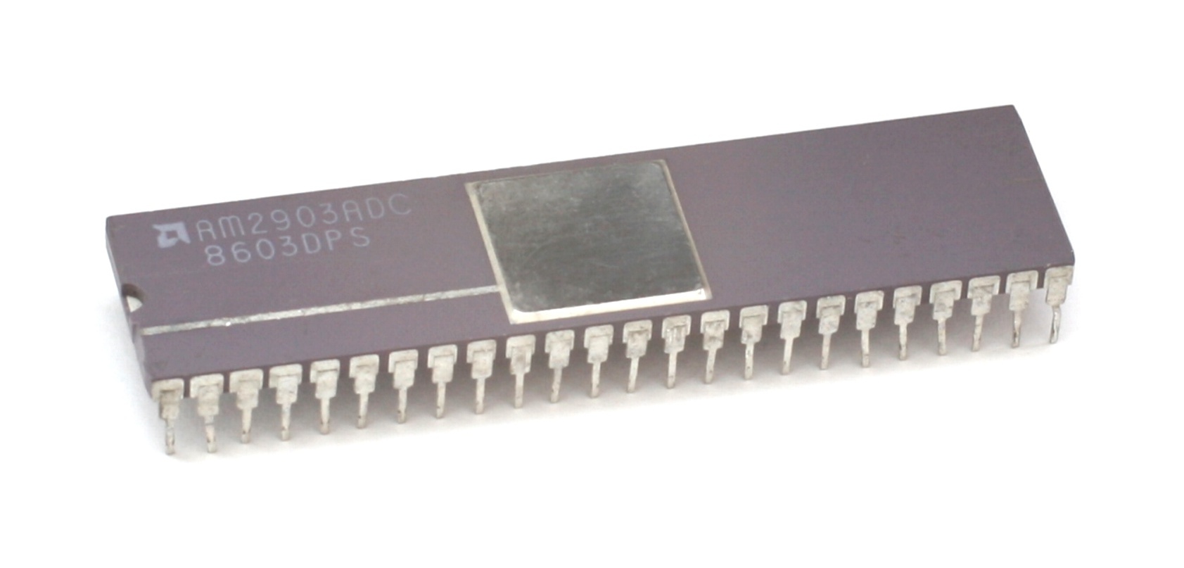
In 1975, AMD created its first two non-licensed processor products. Technically, its AM2900 wasn't a processor; rather, it was a series of components used to build a 4-bit modular processor. It also produced the AM9080, which was a reverse-engineered clone of Intel's 8080 8-bit microprocessor.
Article continues belowThe IBM Agreement
AMD's entry into the x86 processor market began in the early 1980s following an agreement between IBM and Intel. At the time, IBM was one of the largest computer manufacturers in the world and quite possibly the single largest producer of computer products. IBM was deliberating on several different processor designs to use in its upcoming products when it entered into negotiations with Intel. If Intel won the contract, it would secure a massive order for the company's processors for use inside of IBM-compatible PCs.
IBM was concerned, however, that the sheer number of processors that it needed would exceed the production capabilities of any single manufacturer, so it required Intel to license its technology to third-party manufacturers to ensure sufficient total volume. Intel, not wanting to lose the contract with IBM to a competitor, agreed to IBM's terms in 1981.
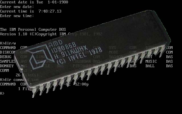
Following the agreement, AMD began producing licensed identical clones of Intel's 8086 processors in 1982.
| Code Name | N/A |
|---|---|
| Release Date | 1982 |
| Architecture | 16-bit |
| Data Bus | 16-bit |
| Address Bus | 20-bit |
| Maximum Memory Support | 1 MB |
| L1 Cache | None |
| L2 Cache | None |
| Frequency | 4 - 10 MHz |
| FSB | 4 - 10 MHz |
| FPU | 8087 (Sold Separate) |
| SIMD | None |
| Fab | 3000 nm |
| Transistor Count | 29,000 |
| Power Consumption | N/A |
| Voltage | 5 V |
| Die Area | 33 mm² |
| Socket | 40 pins |
AM29000 32-Bit RISC Processors
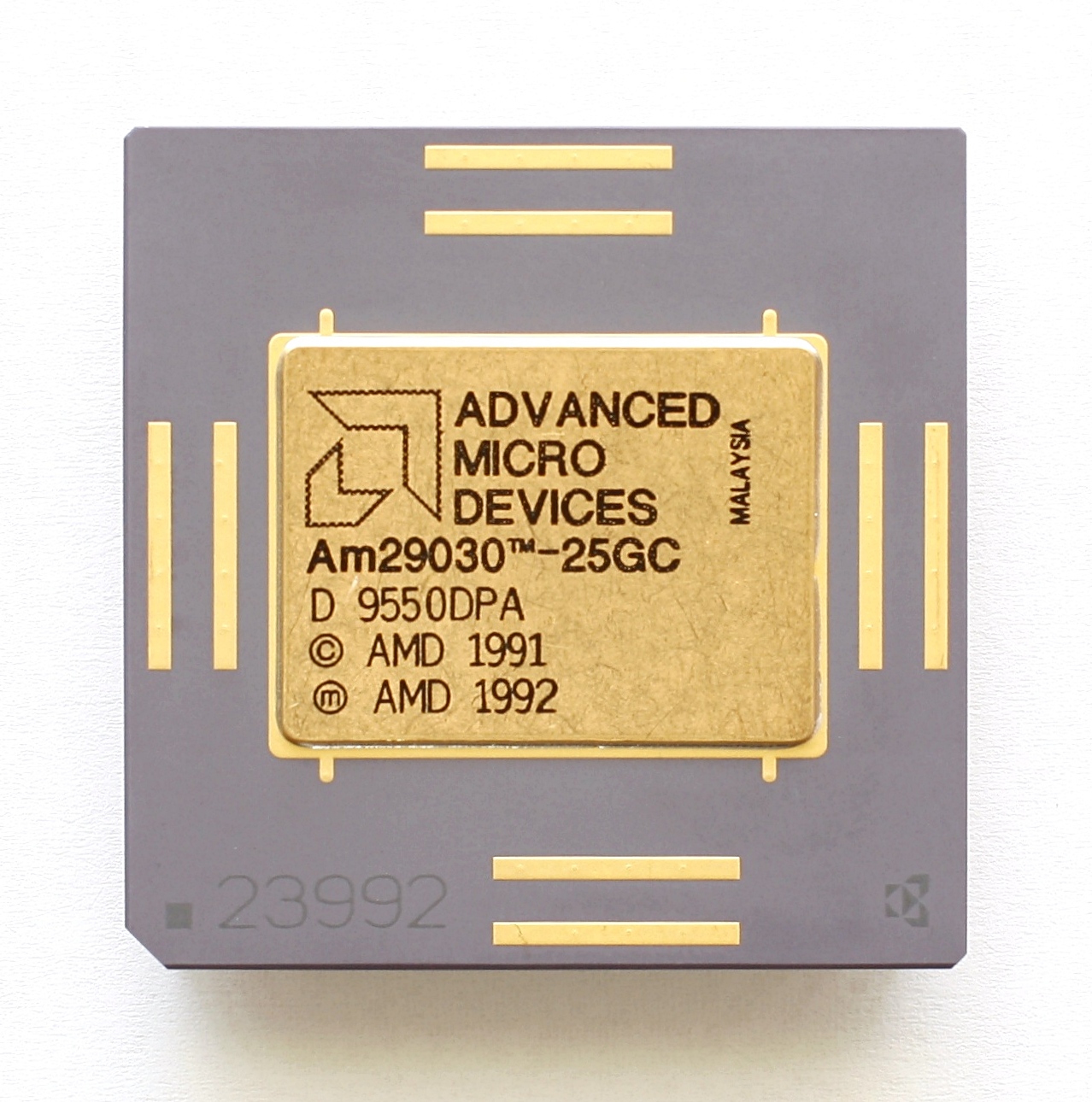
Throughout the 1980s and into the 1990s, AMD also produced a line of 32-bit RISC processors known as the AM29000 series. These processors were essentially the next generation of its earlier AM2900 products, however, and they were targeted more at the embedded market than high-performance computers. AMD designed the AM29000 using a variation of the Berkeley RISC architecture. Eventually, AMD discontinued work on the AM29000 series to focus on its x86 processor line.
Get Tom's Hardware's best news and in-depth reviews, straight to your inbox.
AMD AM286
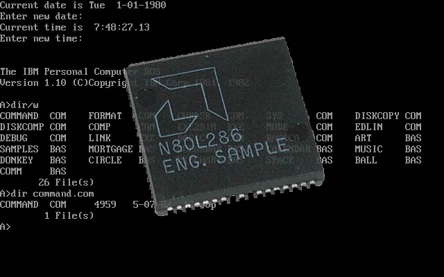
AMD's second x86 processor was the AM286, a licensed clone of Intel's 80286. Although the chip was architecturally identical, it had one advantage over its Intel counterpart: higher clock speeds. Where Intel capped the 80286 at 12.5 MHz, AMD pushed the AM286 as high as 20 MHz.
AMD AM286
| Code Name | N/A |
|---|---|
| Release Date | 1983 |
| Architecture | 16-bit |
| Data Bus | 16-bit |
| Address Bus | 24-bit |
| Maximum Memory Support | 16 MB |
| L1 Cache | None |
| L2 Cache | None |
| Frequency | 8 - 20 MHz |
| FSB | 8 - 20 MHz |
| FPU | 80287 (sold separately) |
| SIMD | None |
| Fab | 1500 nm |
| Transistor Count | 134,000 |
| Power Consumption | N/A |
| Voltage | 5 V |
| Die Area | 49 mm² |
| Socket | 68 pins |
AMD AM386: Legal Battles With Intel
In 1985, Intel released its first 32-bit x86 processor design, the 80386. AMD planned to release its variation, the AM386, not long after, but Intel held it up in court. Intel claimed that its cross-licensing agreement permitted AMD to produce copies of only the 80286 and older processor designs, but AMD argued that the contract permitted it to create clones of the 80386 and future x86 derivatives, as well. After years of legal battles, the courts sided with AMD, and the company was able to release its AM386 in 1991.
Although the AM386 is an 80386 clone, AMD released AM386 processors with clock speeds up to 40 MHz, whereas Intel's 80386 tapped out at 33 MHz. This gave AMD a performance advantage, and as it used the same socket and platform as the 80386, it gave customers an upgrade path to their aging systems.
AMD AM386
| Code Name | N/A |
|---|---|
| Date | 1991 |
| Architecture | 32-bit |
| Data Bus | 32-bit |
| Address Bus | 32-bit |
| Maximum Memory Support | 4 GB |
| L1 Cache | None |
| L2 Cache | None |
| Frequency | 12 - 40 MHz |
| FSB | 12 - 40 MHz |
| FPU | 80387 |
| SIMD | None |
| Fab | 1500 - 1000 nm |
| Transistor Count | 275,000 |
| Power Consumption | 2 W (@33 MHz) |
| Voltage | 5 V |
| Die Area | 42 mm² |
| Socket | 132 pins |
AM486 And AMD 5x86: The Final Clone
The last processor designed by Intel that AMD produced was the AM486 (80486), and it was released in 1994. Due to ongoing legal disputes between Intel and AMD, some versions of the AM486 use Intel microcode whereas others use microcode developed in-house by AMD. AMD followed a similar strategy with its AM486 as it did with the AM386, by pushing clock speed considerably higher than Intel. Although Intel's fastest 80486 processors were capped at 100 MHz, AMD went as high as 120 MHz on the AM486.
Not long after, in 1995, AMD also released its AMD 5x86. This processor used the same architecture as the AM486 and 80486, but it pushed the clock speed even higher. Retail models ran at 133 MHz, and OEMs had access to an even faster 150 MHz version.
Other notable changes in this line of processors was the addition of L1 cache, which helped to increase performance compared to the older 80386/AM386 CPUs. It also moved the FPU into the same package as the CPU, which also significantly improved performance. Prior to this, all FPUs were sold as separate hardware units and connected to the CPU through the motherboard.
Following the release of Intel's first Pentium processor around the same time also lead AMD and other competing CPU designers to introduce the PR or "Pentium Rating" system. This gave companies a simple way to advertise their products against each other and against Intel's Pentium. An example of this is the AMD 5x86 PR 75, which was advertised as having equivalent performance to a 75 MHz Pentium CPU.
AM486 And AMD 5x86
| Code Name | N/A | X5 |
|---|---|---|
| Date | 1993 | 1995 |
| Architecture | 32-bit | 32-bit |
| Data Bus | 32-bit | 32-bit |
| Address Bus | 32-bit | 32-bit |
| Maximum Memory Support | 4 GB | 4 GB |
| L1 Cache | 8 - 16 KB | 16 KB |
| L2 Cache | None | None |
| Clock Speed | 16 - 120 MHz | 133 -150 MHz |
| FSB | 16 - 50 MHz | 33 - 50 MHz |
| FPU | Integrated | Integrated |
| SIMD | None | None |
| Fab | 800 - 1000 nm | 350 nm |
| Transistor Count | 1,185,000 | N/A |
| Power Consumption | N/A | N/A |
| Voltage | 5 V - 3.3 V | 3.45 V |
| Die Area | 67 - 81 mm² | N/A |
| Socket | 168 pins | 168 pins |
K5: AMD's First x86 Processor
In 1996, AMD released its first x86 processor designed entirely in-house. The fifth-generation x86 K5 processor used an innovative design that combined the execution hardware from AMD's discontinued AM29000 RISC processors with an x86 front end. Because the execution back-end hardware was based on a RISC design, instructions were decoded into micro-instructions that could be fed into one of five integer execution units or an integrated FPU.
AMD implemented an out-of-order speculative execution design as well, which helped to boost performance. The overall design was fairly complex, however, which limited AMD's ability to push up the clock speed, and the K5 was not able to surpass Intel's Pentium in terms of performance. It was considered relatively efficient, however, and AMD advertised 100 MHz K5 processors with a PR133 rating, meaning that AMD considered it to have equivalent performance to a 133 MHz Pentium.
AMD K5
| Code Name | SSA/5, 5k86 |
|---|---|
| Date | 1996 |
| Architecture | 32-bit |
| Data Bus | 32-bit |
| Address Bus | 32-bit |
| Maximum Memory Support | 4 GB |
| L1 Cache | 16 KB + 8 KB |
| L2 Cache | None |
| Clock Speed | 75 - 133 MHz (PR75 - PR200) |
| FSB | 50 - 66 MHz |
| SIMD | None |
| Fab | 500 - 350 nm |
| Transistor Count | 4.3 Million |
| Power Consumption | 11 - 16 W |
| Voltage | 3.52 V |
| Die Area | 181 - 251 mm² |
| Connection | Socket 5 & Socket 7 |
K6: AMD's NexGen Processor
Instead of developing a new architecture to succeed the K5, AMD opted to purchase NexGen, a competing manufacturer of processors, and use its upcoming Nx686 design for the K6. Although the design was completely different than the K5, it was somewhat similar at a high level.
For example, like the K5, the K6 also used an x86 front-end to decode instructions into micro-operations that were then executed on internally RISC-like hardware. The K6 was released in 1997, and it was compatible with Socket 7 motherboards; clock-for-clock, it matched the performance of Intel's Pentium II, while also being considerably less expensive. It also included the important MMX SIMD instruction set.
The Pentium II did have one major advantage in that its FPU performance was better than the K6.
AMD K6
| Code Name | K6 (350 nm), Little Foot (250 nm) |
|---|---|
| Date | 1997/1998 |
| Architecture | 32-bit |
| Data Bus | 32-bit |
| Address Bus | 32-bit |
| Maximum Memory Support | 4 GB |
| L1 Cache | 32 KB + 32 KB |
| L2 Cache | None |
| L3 Cache | None |
| Clock Speed | 266 - 350 MHz |
| FSB | 50 - 66 MHz |
| SIMD | MMX |
| Fab | 350 - 250 nm |
| Transistor Count | 8.8 Million |
| Power Consumption | 12 - 28 W |
| Voltage | 2,2 - 3,2 V |
| Die Area | 68 - 157 mm² |
| Socket | Socket 7 |
AMD K6-II
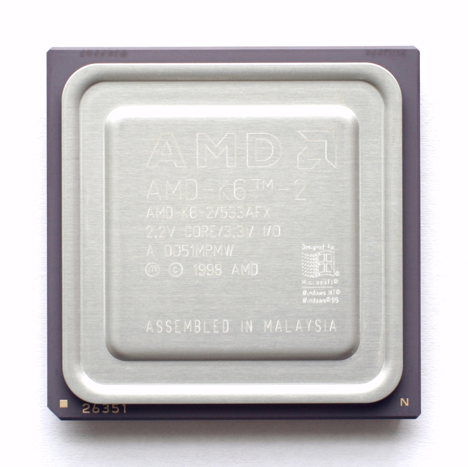
AMD's next processor was the K6-II. It was essentially an extended version of the K6 that could use a faster 100 MHz FSB, higher clock speeds, and new SIMD instructions. AMD introduced its 3DNow! SIMD instruction set as a competitor to Intel's MMX. Similar to AMD's older processors, the K6-II gave customers a clear upgrade path from the aging Pentium MMX processors, and as a result they were highly successful.
AMD K6-II
| Code Name | K6-3D, Chomper |
|---|---|
| Date | 1998 |
| Architecture | 32-bit |
| Data Bus | 32-bit |
| Address Bus | 32-bit |
| Maximum Memory Support | 4 GB |
| L1 Cache | 32 KB + 32 KB |
| L2 Cache | None |
| L3 Cache | None |
| Clock Speed | 300 - 550 MHz |
| FSB | 66 - 100 MHz |
| SIMD | MMX, 3DNow! |
| Fab | 250 nm |
| Transistor Count | 9.3 Million |
| Power Consumption | 13 - 25 W |
| Voltage | 2.2 - 2.4 V |
| Die Area | 81 mm² |
| Socket | Socket 7/Super Socket 7 |
AMD K6-III: Integration Of L2 Cache
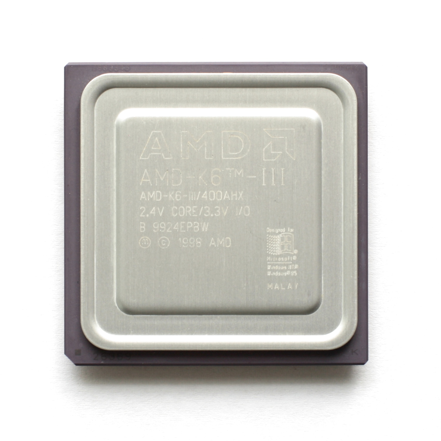
In 1999, AMD released its third-generation K6 processor, the K6-III. It was architecturally similar to the K6 and K6-II, but AMD added 256 KB of L2 cache on the CPU die. Prior to this, L2 was placed on the motherboard and accessed over the FSB, but the tighter integration significantly reduced latency and increased bandwidth. The K6-III was relatively expensive, however, and AMD quickly replaced it with the Athlon processor.
AMD K6-III
| Code Name | Sharptooth |
|---|---|
| Date | 1999 |
| Architecture | 32-bit |
| Data Bus | 32-bit |
| Address Bus | 32-bit |
| Maximum Memory Support | 4 GB |
| L1 Cache | 32 KB + 32 KB |
| L2 Cache | 256 KB (350 - 550 MHz) |
| L3 Cache | None |
| Clock Speed | 350 - 550 MHz |
| FSB | 100 MHz |
| SIMD | MMX, 3DNow! |
| Fab | 250 nm |
| Transistor Count | 21.3 Million |
| Power Consumption | 10 - 17 W |
| Voltage | 2.2 - 2.4 V |
| Die Area | 118 mm² |
| Socket | Super Socket 7 |
-
wurkfur ReplyThe eternal underdog will once more have his day.
How can you say eternal? For a good while AMD was actually making faster and more innovative stuff than Intel.
AMD launched dual cores for consumers
AMD integrated memory controllers on die
AMD created x64 versus Intel pushing the move to a new architecture that only they could make
AMD also pushed APU's mainstream
Intel adopted all these practices after the fact while engaging in illegal monopolistic behavior in an international stage that stifled innovation, cost jobs, and caused consumers to pay more.
One could argue that if Intel had simply played by the rules locally and abroad, AMD would have had enough cash flow to maintain their position through better R&D instead of playing catch up.
For that very reason I look forward to AMD's upcoming products to replace my 1090t that's clocked within an inch of its life. -
vern72 ReplyAMD launched dual cores for consumers
AMD integrated memory controllers on die
AMD created x64 versus Intel pushing the move to a new architecture that only they could make
AMD also pushed APU's mainstream
And one more thing: AMD was the first to ship a 1Ghz x86 CPU to the masses. -
CaedenV Fantastic article! Especially loved seeing the early chips; I had no idea that they were in the game pre 286 generation. I was a kid at the time and my understanding was that the law suits at the time were what allowed AMD (and Via... don't forget the 'true underdog' lol) to ENTER the market, not remain in it.Reply
Also, I remember endless debates when I built my first PC for college ~2001. I wanted an AMD XP chip... but my video editing software had issues with it (some sort of audio processing bug. Then it was between the Pentium 4 which had great burst performance, but terrible sustained performance due to RDRAM that could not keep up; and the Pentium 3 which looked terrible on paper and was 'old', but had fantastic sustained performance (and much healthier thermals!). In the end I decided on the Pentium 3, but (noob build mistake) because I bought a crap PSU it died within a year and I moved to my one and only AMD build which was a 2GHz Barton. That was a great PC that lasted a solid 3 years.
I was really sad to watch Bulldozer fall apart. After the Core2Duo AMD was falling behind and bulldozer was supposed to bring them back into relevance. But then the marketing department thought that nobody would buy a high-end $500+ CPU, so they slashed the cache to make it more affordable. Sadly that cache was needed to prevent the CPU from constantly going back to the system memory for instructions and it literally killed the product. And Intel happily sold several $400-1000 i7 chips while AMD could not even hold onto the budget market. Sad times. It is a shame that they were not able to sell the full chip as originally designed, and then cut down a cheap version for 'consumers'.
But now it looks like AMD is starting to play ball again. Next 3 years will be interesting to watch, and if they make a winner then I might throw my hat in their ring again when I do a rebuild 2-4 years from now. I would love to see something blow my 4.2GHz Sandy Bridge out of the water! -
CaedenV ReplyOld CPUs are so much... cooler than new ones.
you kidding? Those old chips ran meltingly hot! And with tons of power! when those old chips were OC'd they could drink down nearly 200W and easily heat a dorm room on cold winter nights! -
turkey3_scratch Reply17879424 said:Old CPUs are so much... cooler than new ones.
you kidding? Those old chips ran meltingly hot! And with tons of power! when those old chips were OC'd they could drink down nearly 200W and easily heat a dorm room on cold winter nights!
To be fair we have current GPUs on the market above 300W.
But by "cool" I just meant "cool" as in "vintage". -
SinxarKnights It is amazing to think that my old 433Mhz Intel processor was pretty good at the time. With 256MB of RAM the OS (Win98SE) was very responsive. The motherboard didn't have an AGP slot so I had to settle for a Nvidia GeForce FX 5200 from Wal-mart. Still have lots of fond memories of Diablo and Ultima Online.Reply
I built a PC with an Athlon 64 X2 5600+. Due to the larger cache, it gave a significant performance increase over the other lower tiered CPUs. This was right at the time Intel came out with the Core architecture. While the top end 64 X2 series (6000+ and up) outperformed the first Core CPUs that were released, everything went downhill from there for AMD.
15 years ago my awesome 433mhz CPU was awesome, today it cannot perform the most basic of task in a timely manner. I imagine 15 years from now my current 4790k will be in the same boat. -
Zachary Singer-Englar I still brag about my Athlon II x250 Regor. That was a great processor for an underfunded enthusiast, It shipped at 3.0 and i had it clocked to 3.5 for about 2 years on a stock cooler before I replaced the whole set-up because my motherboard gave out (probably unrelated to my overclocking). That was 5 years after I had purchased the processor. My FX-6350 is not holding up quite as well.Reply

