'V-Link'
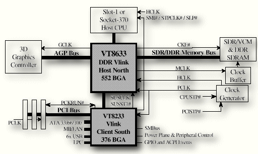
Still VIA has made one major change, which is the interconnection between the 'north bridge' and the 'south bridge' of the Apollo Pro 266 chipset. I have no idea which wise person once invented the names 'north' and 'south' bridge, because your motherboard will actually work just fine even if you point the north bridge to the west and the south bridge to the east. Basically it's a naming that distinguishes the two chips that make up the vast majority of PC chipsets, in which case the 'north bridge' is the chip that hosts the interconnect to the processor, the AGP and the memory, while the 'south bridge' hosts all the other I/O-connections to the hard drive, the USB, serial and parallel ports as well as AC97 sound and modem stuff.
Traditionally, those two chips are using the PCI-bus as their connection, which means that either of those chips has to share this 'highway' with other PCI-devices, such as SCSI-adapters, network cards, sound cards and more. The PCI-bus is 32-bit wide and clocked at 33 MHz, so that the bandwidth that's shared between all those PCI-devices, including north and south bridge, is 133 MB/s.
The introduction of Intel's 810 chipset marked some kind of advance over the above-mentioned old design. Intel's 810 and all other 8xx chipsets are using the lovely-named 'Intel Hub Architecture', which only points out the fact that Intel is now connecting 'north' and 'south' bridge via a dedicated little bus that is 8-bits wide, but double-pumped and clocked at 133 MHz, providing an unshared band width of 266 MB/s between the two chips. The PC-bus is in this case only connected to the 'south' bridge, or as Intel names it, the 'ICH' = I/O Controller Hub.
What Intel can do VIA finally figures out as well and so Apollo Pro 266 is now the first chipset with a solution that's virtually identical to Intel's 'hub architecture', but with the name 'V-Link' not baptized half as kewl . It's hard to beat Intel's marketing department, wouldn't AMD know that as well?
The average computer user will not notice any difference between the 'old' PCI-bus solution and the new 'hub architecture' or 'V-Link' architecture, but once you remember how high the data bandwidth of PCI devices such as IEEE1394, SCSI-3 or the next ATA-solution can actually get you might feel a bit safer with the new 266 MB/s interconnect.