Intel's Slot 1 CPUs Uncovered
The Pentium II 400 Is Using The 82459AD Tag RAM Module

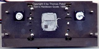
This is the back plate of a Pentium II 333 to which you mount the heat sink on the other side. You can see the thermal grease where it fits onto the Deschutes core. There are no special notches left and right of it.

The back plate of a Pentium II 400 looks quite a bit different. The bottom part is also aluminium, not an extra plastic part as removed in the picture of the Pentium II 333 back plate. You can easily spot the two notches for the L2 cache modules, both covered with thermal grease. Intel Celeron, Core Codename Deschutes
The Celeron, Intel's attack on the CPU suppliers of the low end market, comes with the same 0.25 micron core as the Deschutes and is therefore 'more modern' than the Pentium II 233-300 CPUs with their 0.35 micron Klamath core. Celeron has not got any L2 cache and is otherwise identical to the other Pentium II CPUs. Thus is can show its strengths when running floating point calculation intensive applications like 3D games in the first instance, a field where it is faster than any currently available socket 7 CPU. The lack of L2 cache results in a decent but not amazing office application performance, but it has got it's advantages as well. As you learned from the stuff above, the L2 cache is making the most trouble when clocking the Slot 1 CPUs higher. The Celeron doesn't have to worry about that. Only it's successor with the codename 'Mendocino' will have an internal L2 cache and will hence be more sensitive to higher clock speeds as well. The just said leads to the simple conclusion that only the core is responsible for the success in overclocking the Celeron. Now the sweet thing about the Celeron is the fact that it's using the Deschutes core, as already mentioned. This core was designed to run at least 333 MHz as in the Pentium II 333. The 0.35 micron Klamath is already reaching 300 MHz without a problem, so that you can imagine that you will hardly find a Deschutes core that doesn't at least do 333. These cores are used in a Celeron and the Celeron is specified to 266 MHz only to not damage the sales of the Pentium II 233, not because the core wouldn't be fast enough. So here we are, Celeron is the number one overclocking CPU and if you should run it fast enough, you can even reach Pentium II 350 scores, particularly in 3D games as Quake II, but by paying less than a third for it. The problem for overclocking is that you will need a BX board that doesn't detect the FSB clock automatically, so that you can run this baby at 100 MHz FSB.
The Celeron comes as naked as Andy created him (before he handed over). No plastic cartridge covers the PCB and the heatsink that comes with it has to be fixed in a slightly annoying procedure. Intel was trying at least a little to keep people from plugging Celeron into LX or BX boards. The little mounting brackets which fit nicely in any EX board wouldn't fit at all into LX or BX boards. MSI is only one of the motherboard manufacturers who told me their plans on working around that. Until then you shouldn't play football with your computer after plugging the Celeron in your LX or BX board, because you won't be able to secure the Celeron in Slot 1. This is important for people in earth quake endangered areas.

There isn't much more than the CPU core on the PCB of Celeron. Please note that you won't find the R5/R6 resistors as in Deschutes for allowing it 100 MHz FSB officially. The Celeron is meant to be running at 66 MHz FSB only, so B21 is hardwired to Low.

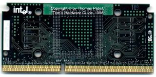
There isn't much to say, the back side of the Celeron is simply empty.
Note: 'PCB' stands for 'printed circuit board'.
Stay On the Cutting Edge: Get the Tom's Hardware Newsletter
Join the experts who read Tom's Hardware for the inside track on enthusiast PC tech news — and have for over 25 years. We'll send breaking news and in-depth reviews of CPUs, GPUs, AI, maker hardware and more straight to your inbox.
Current page: The Pentium II 400 Is Using The 82459AD Tag RAM Module
Prev Page The Common Core Voltage Of The Deschutes Core Is 2 VMost Popular


