World’s Largest 3D Photonic Quantum Chip Boosts Quantum Simulation Performance
Get Tom's Hardware's best news and in-depth reviews, straight to your inbox.
You are now subscribed
Your newsletter sign-up was successful
A research team from the Shanghai Jiao Tong University in China announced that it has developed the world’s largest 3D photonic quantum chip that can demonstrate a 2D quantum walk and boost the performance of quantum simulation.
Quantum Walks
A quantum walk is analogous to a classical random walk (succession of random steps), except the walker in a quantum walk is in a superposition of positions. That means the walker could be in all of the positions at the same time.
What this means in practice is that a quantum walk can show superior performance to classical random walks for quantum searching and quantum simulation applications. Previously, most experimental quantum work was in one dimension, but now it can be done in more dimensions.
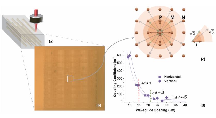
Article continues belowThe STJU team used a technique called “femtosecond laser direct writing” to construct a 3D photonic chip with up to 49x49 nodes, making it the world’s largest-scale chip ever. Using this chip, the team was able to demonstrate a 2D continuous-time quantum walk in real spatial space.
The STJU team’s work should pave the road for the development of quantum algorithms based on quantum walks, as well as easier and more complex quantum experiments in the future.
Accelerating Towards Practical Quantum Computers
Over the past few years we’ve seen not just more universities but also companies such D-Wave, Google, IBM, Intel, Microsoft, Rigetti, and others, as well as governments starting to double down on quantum computers, working on and investing in quantum computing research.
Quantum computers promise to aid in the discovery of major breakthroughs in science and medicine and solve many other significant world problems, which couldn’t be easily solved with classical computers.
Get Tom's Hardware's best news and in-depth reviews, straight to your inbox.
Lucian Armasu is a Contributing Writer for Tom's Hardware US. He covers software news and the issues surrounding privacy and security.
