AMD Puts Hopes on Packaging, Memory on Logic, Optical Comms for Decade Ahead
Advanced architecture and packaging will make up for tapering process technology benefits.
At the ISSCC 2023 earlier this week, AMD discussed the future of computing over the next decade. CEO Dr. Lisa Su was the lead presenter and showed that AMD has performed admirably in supercomputer, server, and GPU performance trends over the last few decades. However, probably more interesting are the well-crafted plans that show how AMD aims to keep the pedal to the metal and use advanced technologies to counteract the tapering off of semiconductor process shrink benefits.
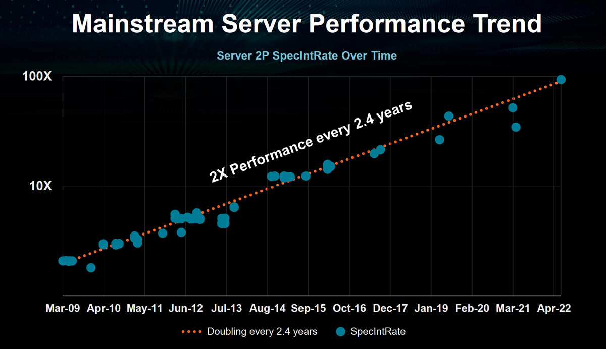
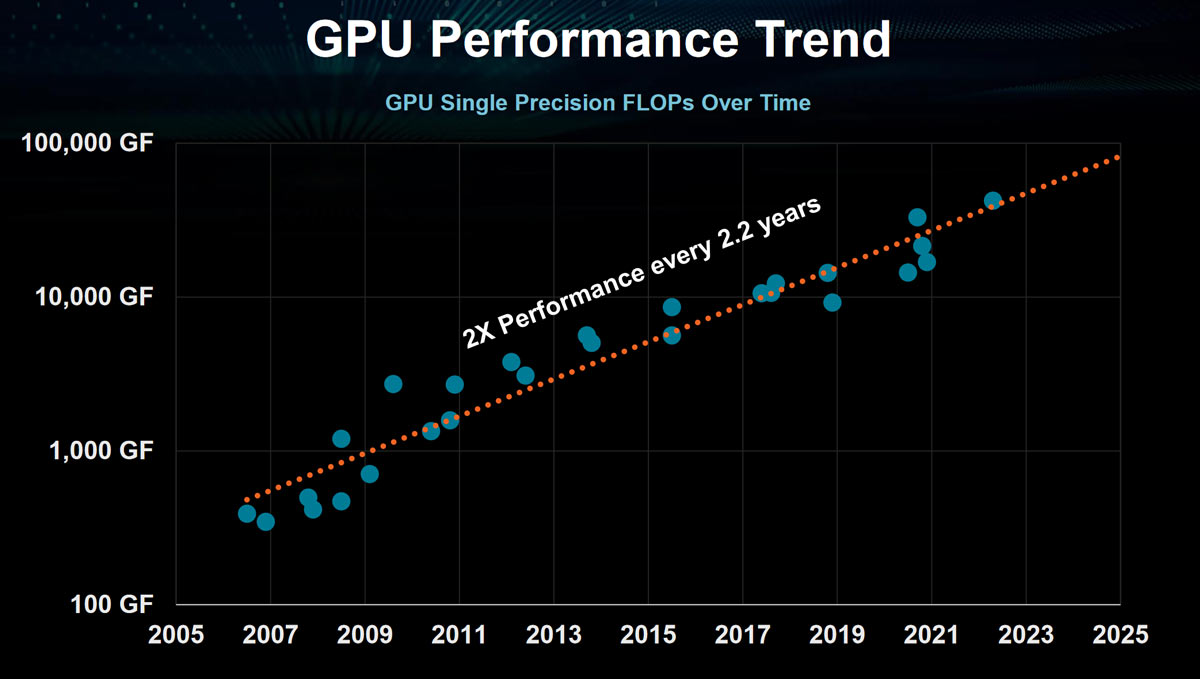
In the above performance slides, AMD claims it has successfully doubled mainstream server performance every 2.4 years since 2009. However, it doesn’t share any projections with respect to this market. AMD is confident to peer further into the future with its GPU performance trends (slide 2 in the gallery above). Here you can see that it claims to have doubled GPU performance every 2.2 years since 2006. The chart shows this trend is locked in until at least 2025.
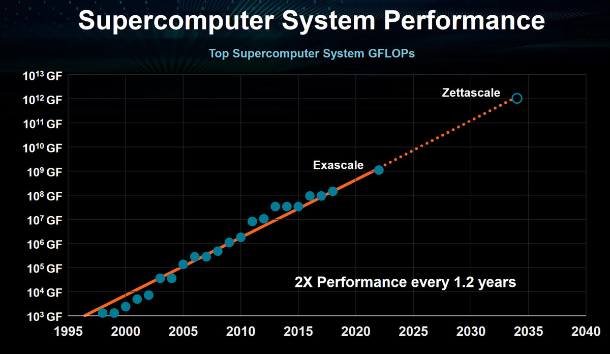
AMD's supercomputer performance is the most successful in terms of advances over time, with the last chart above showing that, since the late 90s, AMD processors have been instrumental in doubling supercomputer performance every 1.2 years. Moreover, AMD predicts we will reach Zetascale supercomputer performance in approximately a decade. AMD also took time to highlight efficiency gains, and the intense battle to keep Moore’s Law alive as logic density tapers off.
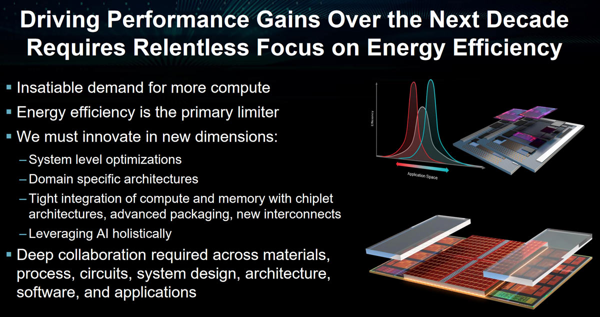
Generously, AMD laid out some of its key plans which will help it drive forward with efficiency and performance gains over the coming decade. Advanced packaging is going to be a strong driver of both performance and efficiency, according to AMD. We have already seen some of the results of AMD traveling down this path with the use of chiplets and 3D V-Cache, and it will continue.
Article continues below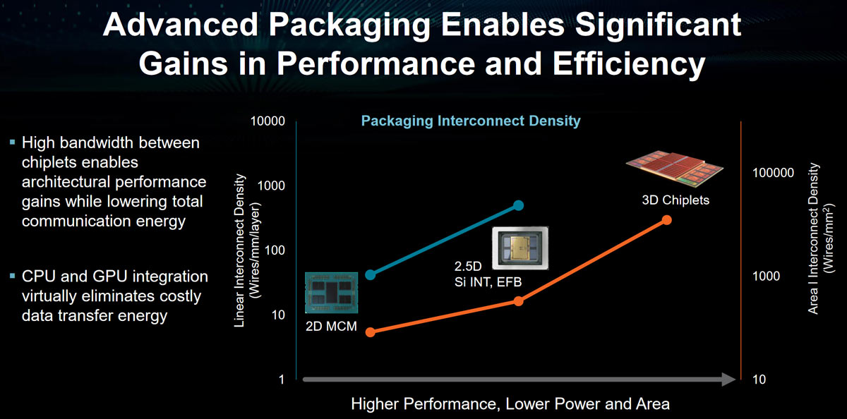
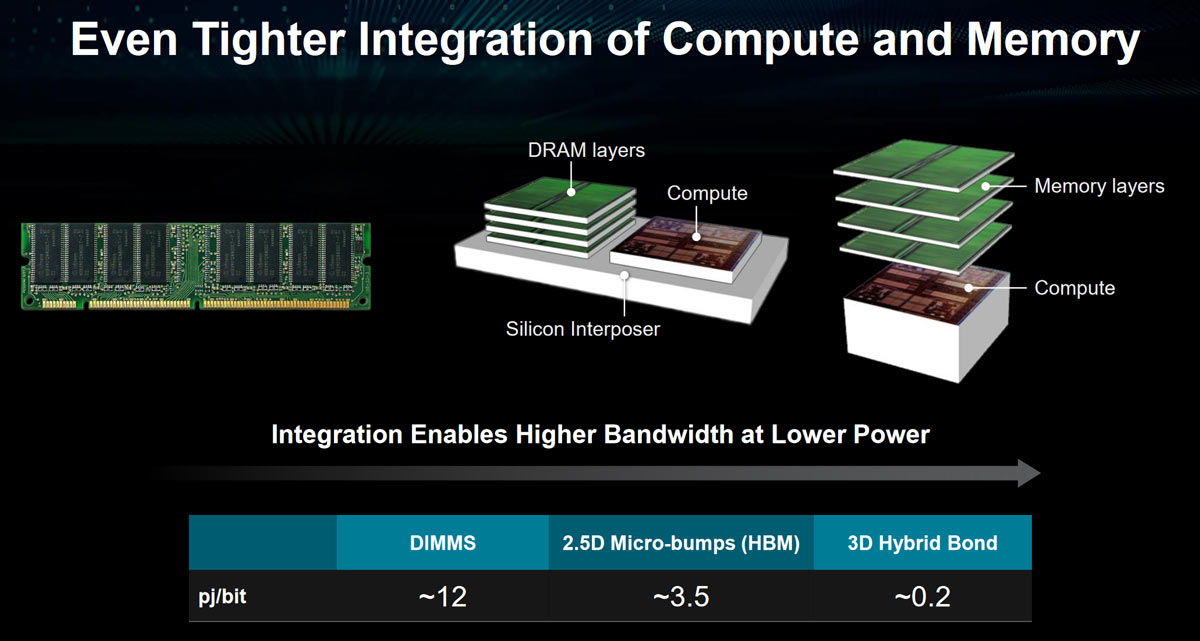
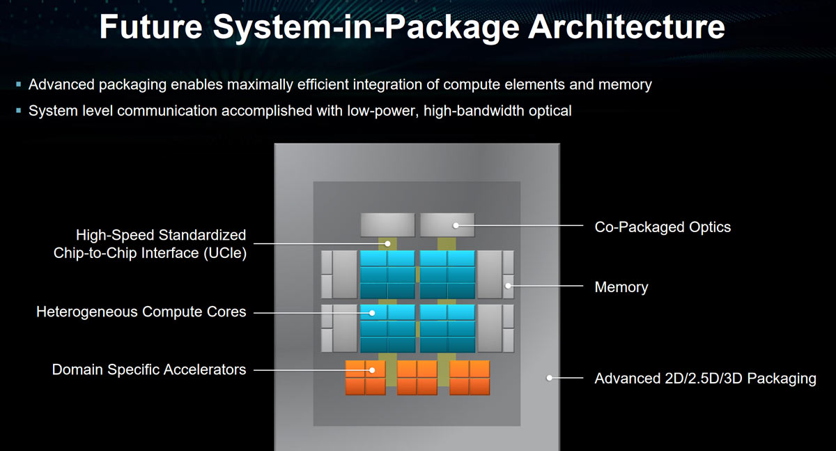
Some advanced packaging avenues which will be explored include the integration of 3D CPU & GPU silicon “for next-level efficiency.” Additionally, AMD reckons that “even tighter integration of compute and memory” will result in higher bandwidth with lower power. AMD will also target processing in memory. A slide shared at ISSCC showed a processor with an HBM module stacked on top. AMD says that if key algorithmic kernels can be executed in memory, that takes significant burden and latency out of the system.
Another big target for efficiency savings, and thus potential performance boosts, are chip I/O and communications. Specifically, using optical communications tightly integrated with the compute die is expected to provide a worthwhile efficiency boost.
AMD also took some time to boast about the AI performance gains which have been delivered by its processor portfolio over the last decade. The presentation discussed some use cases for AI computing and highlighted the potential performance gains AI can deliver for simulations.
Of course, AMD isn’t alone in looking at the benefits of advanced packaging, chiplets, die stacking, in-memory computing, optical computing, and AI acceleration. It is good, though, to see that it has solid plans for fierce competition with rivals, and to produce ever faster and more efficient chips for PC enthusiasts.
Get Tom's Hardware's best news and in-depth reviews, straight to your inbox.

Mark Tyson is a news editor at Tom's Hardware. He enjoys covering the full breadth of PC tech; from business and semiconductor design to products approaching the edge of reason.
-
usertests A further 10x performance/watt (efficiency) should be easily achievable. They want upwards of 200-1,000x within the next 15 years or so to enable zettascale supercomputers, and it might be possible to go further than that with 3D packaging.Reply
Computing has already come so far, but adding a few more zeroes to the end could make things comical. -
InvalidError The CPUs with on-package if not direct-stacked memory that I predicted about two years ago are one more step closer.Reply
I wouldn't be surprised if DDR6 ends up being the last external memory standard we get before main memory moves on-package and external memory expansion when you need more than whatever on-package memory your CPU/GPU has goes PCIe/CXL.
An IGP chiplet/tile with 4-8GB of stacked HBM-like memory and almost direct access to the system memory controller should be interesting. -
bit_user Weird that they wouldn't plot Genoa on here:Reply
Maybe it blows up their nice trend, with that massive 1.5x core-count increase and DDR5 memory?
I also wonder what SPECint they used... did they go back and re-test old Opteron servers with SPEC2017?
AMD will also target processing in memory.
This should set the stage for an interesting battle with Samsung and SK Hynix, both of which have been very active in this space. If it's truly core to AMD's strategy, I doubt they'll be content to source PIM solutions from partners.
Can someone explain the difference between "2.5D Si INT, EFB" and "3D Chiplets", in the first slide of the second set?
And, on the next slide in that set, how much should we read into the subtly different wording: "DRAM layers" vs. "Memory layers"?
Another big target for efficiency savings, and thus potential performance boosts, are chip I/O and communications. Specifically, using optical communications
How much latency would these optical transceivers tend to add?
AMD also took some time to boast about the AI performance gains which have been delivered by its processor portfolio over the last decade.
Nvidia still owns this market. If AMD really wants to play ball, they need to do a better job of hardware support across their entire stack, making it easy for even novice users to use any AMD GPU for AI acceleration.
And then they need to design hardware that's 2 generations ahead of where they think Nvidia will be, because that's where they will actually be, when AMD launches it product. For too long, AMD's AI performance has been a generation behind Nvidia's. That's because Nvidia understands it's truly strategic, whereas AMD treats it as a "nice-to-have". However, the hardware doesn't even matter if the software support & mindshare isn't there. -
bit_user This slide places too little emphasis on software, IMO.Reply
In particular, programming models will need to shift. Caches are a great way for speeding up software without breaking backward-compatibility, but the lookups burn a lot of power. I think we will need to start reducing dependence on hardware-managed caches. Hardware prefetchers are also nice, but have their own overheads and limitations.
Finally, I keep expecting the industry to start looking beyond conventional approaches to out-of-order execution. We can't go back to strictly in-order, but I think there's a better compromise than the current conceit of a serial ISA that forces the hardware to do all the work needed to find concurrency. -
InvalidError Reply
2.5D is when you use interposers to tie different dies together a bit like current-day HBM, 3D is when stuff gets stacked directly on top or tucked under some other major function silicon instead of dedicated interconnect silicon.bit_user said:Can someone explain the difference between "2.5D Si INT, EFB" and "3D Chiplets", in the first slide of the second set?
So AMD's 3D-Vcache products are basically a mix of 2.5D to connect chiplets and 3D for the extra cache directly on CPUs.
Since AMD spun off the cache and memory controllers into chiplets for its higher-end GPUs, the logical evolution would be for the cache-memory controllers to become the base die for some sort of HBM-like memory.
Going "pure 3D" may be problematic since heat produced closer to the BGA/LGA substrate has to travel through everything stacked on top to reach the IHS or heatsink. Anything besides low-power stuff where this isn't an issue will likely remain hybrid 2.5-3D for thermal management reasons. -
bit_user Reply
Well, if you look at the slide, the starting point seems to be chiplets, since they show a picture of a de-lidded EPYC. So, I assume "2.5D Si INT, EFB" means more than that.InvalidError said:2.5D is when you use interposers to tie different dies together a bit like current-day HBM,
I wonder if they could integrate graphene to wick away heat from the compute layer.InvalidError said:Going "pure 3D" may be problematic since heat produced closer to the BGA/LGA substrate has to travel through everything stacked on top to reach the IHS or heatsink. Anything besides low-power stuff where this isn't an issue will likely remain hybrid 2.5-3D for thermal management reasons.
https://arxiv.org/ftp/arxiv/papers/1503/1503.01825.pdf
"Compared with metals or semiconductors, graphene has demonstrated extremely high intrinsic thermal conductivity, in the range from 2000 W/mK to 5000 W/mK at RT. This value is among the highest of known materials. Moreover, few-layer graphene (FLG) films with the thickness of a few nanometers also maintain rather high thermal conductivity unlike semiconductor or metals. Therefore, graphene and FLG are promising materials for micro or even nanometer scale heat spreader applications"
You might use some TSV approach to send the heat up to the top of the stack, or maybe the entire package is a vapor chamber and you'd just have to draw the heat out to the edges of the chip.
Or, why would the compute die need to be at the base of the stack? Why couldn't it sit on top? Especially if it were restricted to computing on just the memory within the stack, then you might not need so many I/Os between it and the rest of the package. -
InvalidError Reply
I'd imagine that sending 100-250A through bottom dies' with a helluva bunch of TSVs would make burying DRAM, SRAM, NAND and other dense structures under a CPU/GPU die kind of problematic. Thermal vials through silicon would be a no-go for the same reason. Much simpler to limit TDP to what the stack can pass.bit_user said:Or, why would the compute die need to be at the base of the stack? Why couldn't it sit on top?
Using a graphene heat-spreading layer between 3D-stack layers might help alleviate hot spots and improve heat propagation through the stack, though I bet we are 10+ years away from economically viable ways of doing that for consumer electronics. Since graphene is an extremely good electrical conductor, the heat-spreading graphene layers would need to have thousands of holes precision-cut out of it to avoid interfering with copper pillars between dies, can't imagine that getting cheap any time soon. -
JamesJones44 ReplyInvalidError said:The CPUs with on-package if not direct-stacked memory that I predicted about two years ago are one more step closer.
I wouldn't be surprised if DDR6 ends up being the last external memory standard we get before main memory moves on-package and external memory expansion when you need more than whatever on-package memory your CPU/GPU has goes PCIe/CXL.
An IGP chiplet/tile with 4-8GB of stacked HBM-like memory and almost direct access to the system memory controller should be interesting.
Yep, I figured once Apple pushed putting memory on die in the name of efficiency and it was successful, at some point the general PC community would follow for the same reasons. -
Kamen Rider Blade Reply
It's the eventual push for tiering of more Memory Layers.JamesJones44 said:Yep, I figured once Apple pushed putting memory on die in the name of efficiency and it was successful, at some point the general PC community would follow for the same reasons.
If you thought what we have now is crazy, there will be more layers of memory added in the future.
L4$/L5$/L6$/L7$ will all have their place.
