AMD Transitioning To 12nm LP Process For Vega, Ryzen In 2018
At the Global Foundries Technology Conference, AMD’s CTO Mark Papermaster announced that the company will be transitioning “graphics and client products” from the Global Foundries 14nm LPP FinFET process it uses today to the new 12nm LP process in 2018. Global Foundries also announced that 12LP will begin production in 1Q18.
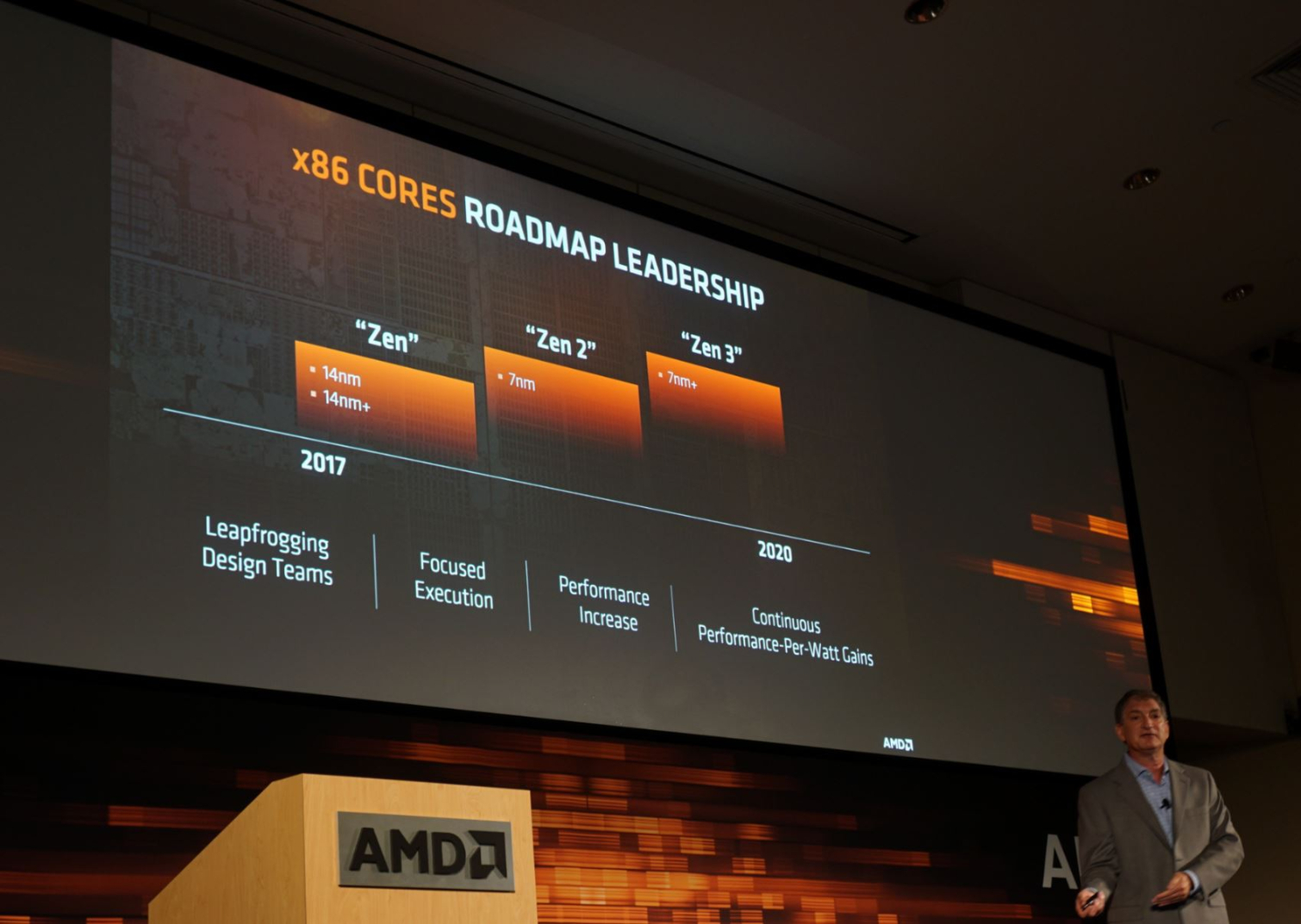
We followed up with Papermaster in person and confirmed directly that the company will transition both Vega GPUs and the Ryzen line of processors to the 12nm LP process. However, it’s still not clear whether or not he meant that 12nm LP will be a shrink of Ryzen in 2018 (a "tick" equivalent if you will) or if Zen+/Zen 2 will also be using the 12LP process. Previously, AMD has implied that Zen 2 will use the 7nm process. The company has used both "Zen+" and "Zen 2" to refer to its next-generation die.
We expected AMD's next-generation 7nm Zen products to slug it out with Intel's 10nm Ice Lake processors next year, but it appears we will see 12nm LP against Intel's 10nm instead.
Article continues belowEarlier, we learned from Raja Koduri's letter to his team that we should expect "new wave of product excitement" in early 2018, which implies that is when we might see the first news of Vega with the 12nm LP process to emerge.
Nvidia’s Volta architecture is already shipping on TSMC’s 12nm FFN process this year, so on the GPU side Nvidia seems to be ahead on adopting new process technology right now. Of course, on the CPU side we also have Intel, which promised “real” 10nm chips for next year that should also be significantly ahead in performance and power efficiency compared to the 12LP process.
However, this is nothing really new, as Intel has been ahead in process technology for quite some time, and if anything, third-party foundry companies such as Samsung/Global Foundries and TSMC have closed the gap a little once they adopted the FinFET structure for their transistors. AMD's relatively quick transition to the 12nm LP processor is vital for the company as it seeks to compete with Intel's Coffee Lake processors and Nvidia's Volta GPUs.
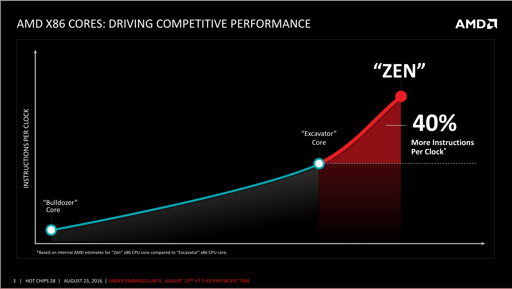
MORE: Everything Zen: AMD Presents New Microarchitecture At Hot Chips
Get Tom's Hardware's best news and in-depth reviews, straight to your inbox.
The transition to 12nm LP also reaffirms AMD's commitment to its partnership with Global Foundries. The companies signed a five-year wafer supply agreement recently, but there has been speculation that AMD might seek other partners for its forthcoming product generations.
We're digging in deeper for more information and will follow up as required.
Lucian Armasu is a Contributing Writer for Tom's Hardware US. He covers software news and the issues surrounding privacy and security.
-
AgentLozen This article says that AMD is shrinking Ryzen and Vega for 2018. I've read in the past that they plan to integrate those two chips together to make a successor to their hybrid CPU line.Reply
If that was the case, can Vega use DDR4 system memory when it was designed for HBM2? As an engineer, do you just swap out the memory controllers and you're good to go? -
gparmar76 I'm assuming the APU Raven Ridge won't use HBM unless it's integrated on die...either way, it'll be light-years ahead of Intel's onboard graphics.Reply -
TJ Hooker Reply
Vega is the codename for the particular piece of silicon powering Vega 56/64. The underlying mico-architecture of Vega is GCN 5th Gen, and I don't see why they wouldn't be able to use it with alternate memory types.20193660 said:If that was the case, can Vega use DDR4 system memory when it was designed for HBM2? As an engineer, do you just swap out the memory controllers and you're good to go?
For example, GCN 3rd Gen was used in Tonga (R9 285, 380(X) w/ GDDR5), Fiji (Fury (X)/ Nano w/ HBM), and Bristol Ridge APUs (DDR4). -
gparmar76 Reply20193812 said:
Vega is the codename for the particular GPU powering the Vega 56/64 graphics cards. The underlying GPU architecture of Vega is GCN 5th Gen, and I don't see why they wouldn't be able to use it with alternate memory types. For example, GCN 3rd Gen was used in Tonga (R9285, 380(X) w/ GDDR5), Fiji (Fury (X)/ Nano w/ HBM), and Bristol Ridge APUs (DDR4).20193660 said:If that was the case, can Vega use DDR4 system memory when it was designed for HBM2? As an engineer, do you just swap out the memory controllers and you're good to go?
Yes but wasn't the new architecture designed for HBM? The onboard graphics CPU from AMD uses DDR4 system memory which is slower than HBM...I'm also curious if there will be any memory on die dedicated to the graphics chip...if not, will performance be much lower using DDR4?
-
drtweak What amazes me is that when I REALLY got into PC's the PIII just came out. To think that was 250nm and now here we are talking about 7nm. all this in less than 20 years.Reply -
gparmar76 Reply20193827 said:What amazes me is that when I REALLY got into PC's the PIII just came out. To think that was 250nm and now here we are talking about 7nm. all this in less than 20 years.
Yeah technology moves damn fast...makes me wonder why reprogrammable CPUs haven't been explored... imagine being able to recode older CPUs with newer instructions...that could extend the life of a CPU for many years...I do believe Intel explored this possibility but it was abandoned pretty quickly.
-
junglist724 Reply20193660 said:This article says that AMD is shrinking Ryzen and Vega for 2018. I've read in the past that they plan to integrate those two chips together to make a successor to their hybrid CPU line.
If that was the case, can Vega use DDR4 system memory when it was designed for HBM2? As an engineer, do you just swap out the memory controllers and you're good to go?
Vega's high bandwidth cache controller can already directly access system ram, and potentially storage, or even other pci-e devices. There's also already a Vega professional card coming that has 2TB of onboard NAND flash connected via AMD's infinity fabric. -
TJ Hooker Reply
That's basically what an FPGA is (or rather, something that an FPGA could do), and they've been around for decades. Intel somewhat recently bought Altera (major FPGA producer), and I believe they are planning on (or already have) put FPGAs into some of they're Xeon processors.20193839 said:Yeah technology moves damn fast...makes me wonder why reprogrammable CPUs haven't been explored... imagine being able to recode older CPUs with newer instructions...that could extend the life of a CPU for many years...I do believe Intel explored this possibility but it was abandoned pretty quickly.
But that doesn't magically extend the life of the CPU. You're still stuck on the same process (meaning same or similar clock speeds) with the same number of transistors. You could in theory reprogram parts of the FPGA to provide hardware acceleration for very specific tasks (which I believe is the idea behind the FPGA module on Xeons), but you can't just reconfigure the whole thing and get a faster CPU out of nowhere. Also, I'm pretty sure the FPGA required to implement a contemporary CPU would be much more expensive than the regular CPU would be. -
photonboy A "vega + Zen" APU would not contain any large amount of memory. You can't simply add HBM memory then expect things to work properly with modern Operating Systems like Windows.Reply
It's also a BUDGET solution anyway since the amount of GPU die space is limited so it makes no sense to increase the cost.
Now for MOBILE devices that have no memory expansion it MAY make sense to use an APU or SoC (system on chip) that has HBM memory acting as a shared CPU/GPU memory though I suspect there's no current market for that approach -
photonboy Also Vega's HBM controller is NOT the same idea as having fast, close memory to the APU. That's a lot of added latency to talk to something much slower, so the SOFTWARE for the program must be designed to work with it to swap data to and from slower memory to shared system memory in a logical way.Reply


