Hot Chips 2017: A Closer Look At Nvidia's Volta
Get Tom's Hardware's best news and in-depth reviews, straight to your inbox.
You are now subscribed
Your newsletter sign-up was successful
Hot Chips is a yearly conference where the best and the brightest of the semiconductor industry provide deep-dive details on the latest cutting-edge processors. This year featured a diverse range of topics that mirror the latest industry trends. Naturally, that means a huge dose of AI. Presentations from Nvidia, Google, and Microsoft, among many others, outlined the latest developments.
Nvidia was on hand to present some of the finer microarchitectural details off its new Volta GV100 SMs. We'll get to the presentation shortly, but we also had a meeting with Rob Ober, Tesla Chief Platform Architect at Nvidia, for a closer look at the GV100.
Nvidia Volta GV100
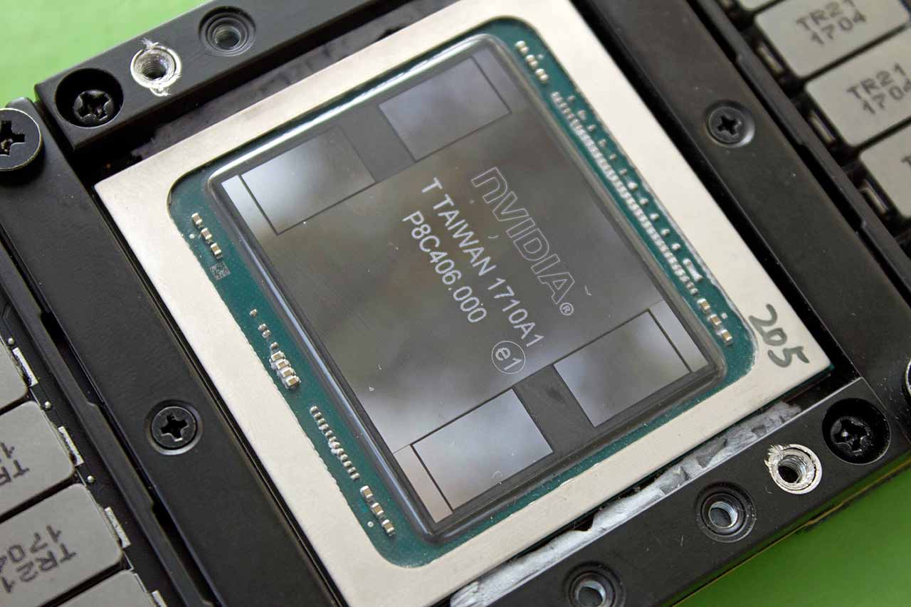
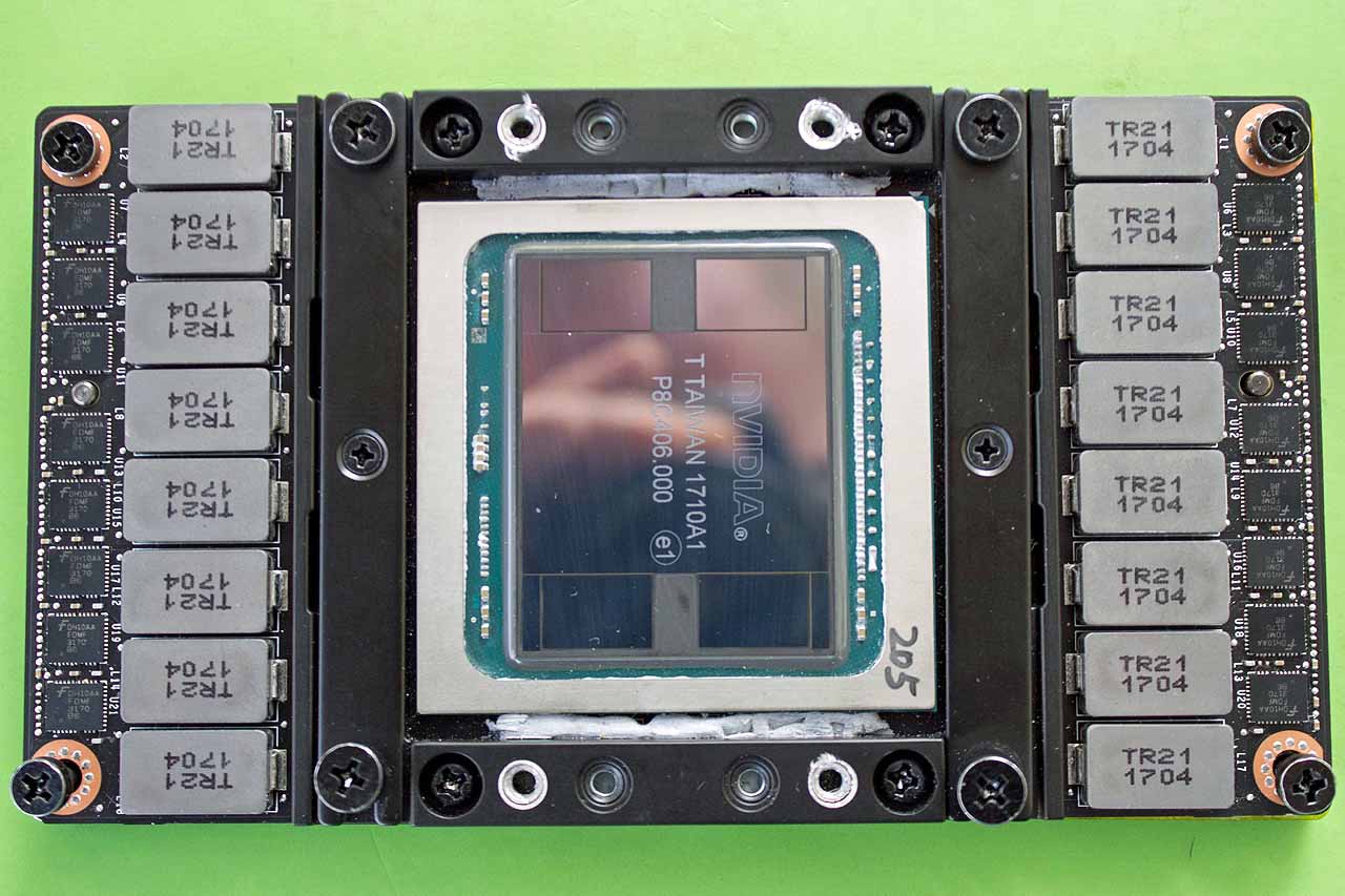
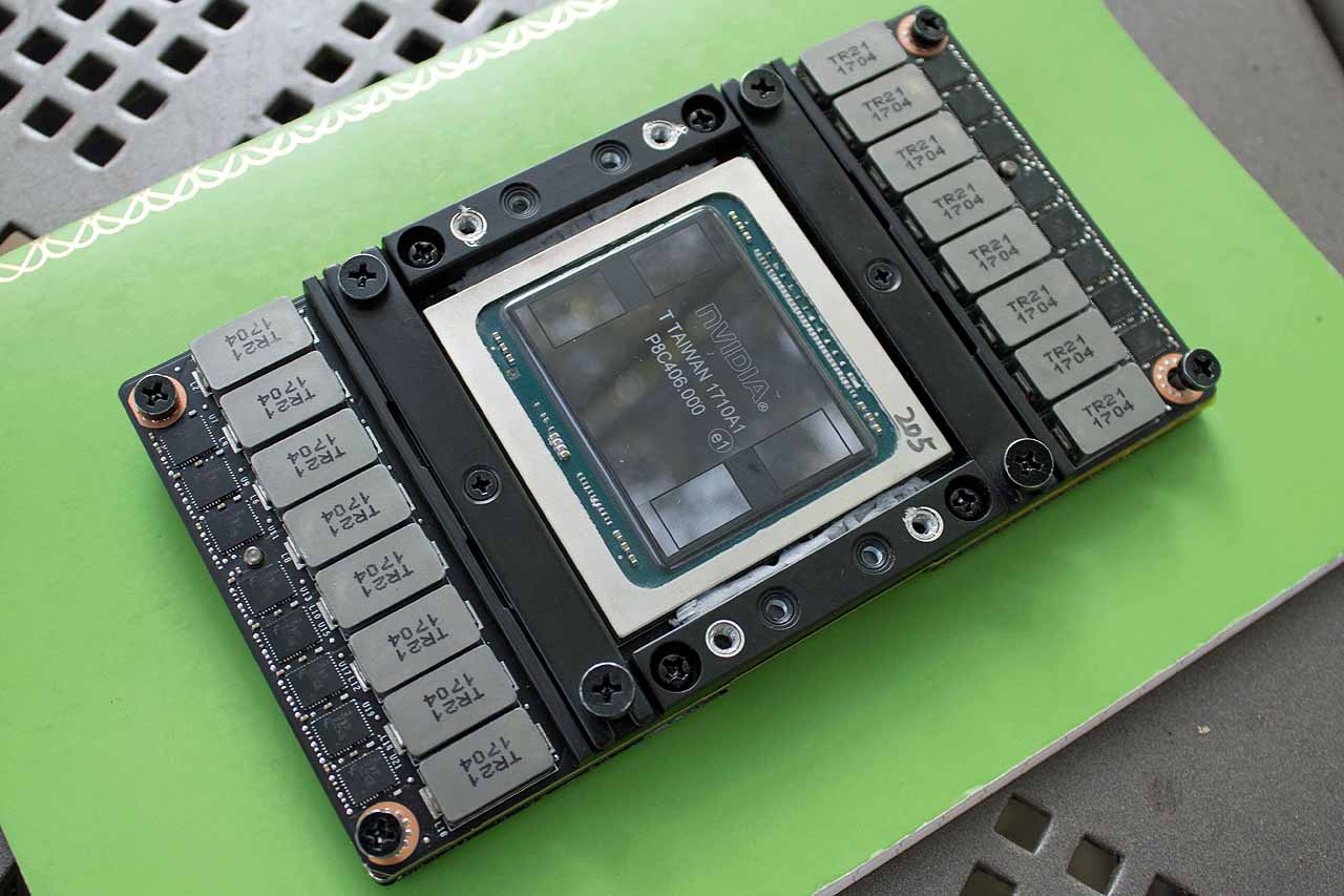
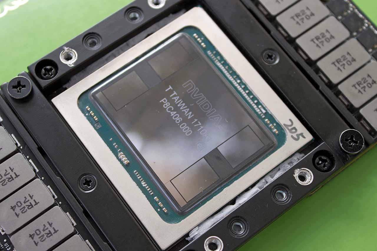
Ober happened to have a Tesla V100 tucked away in his bag, so we took the opportunity to snap a few pictures. The GV100 comes in the SXM2 form factor. Four stacks of HBM2 (16GB total) ride on a silicon substrate carrier, visible on opposing sides of the die, and they're flanked by four "wings" that help support the package when heatsink mounting pressure is applied.
Article continues belowNvidia is pushing the boundaries of semiconductor manufacturing with Volta; it's the company's largest die yet. The massive 815mm2 Volta die, which wields 21 billion transistors built on TSMC's 12nm FFN process, is almost the size of a full reticle. That presents challenges due to the high probability of defects.
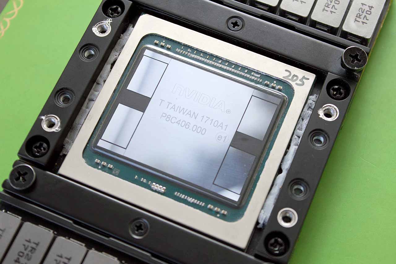
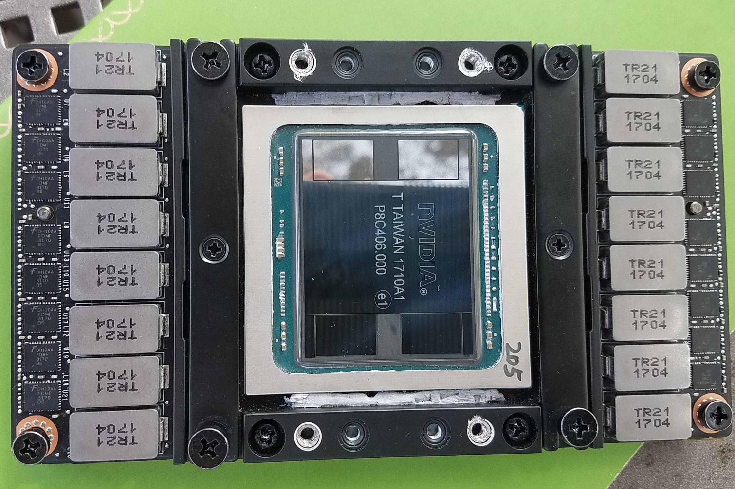
Nvidia ships the GPU with 80 activated SMs (5,120 CUDA cores), but the company designed the die with 84 SM to maximize yields. The four spare SMs offset any defects in the manufacturing process; the probability of one SM suffering from a defect is high, whereas the chances of four defective SMs is quite low. Nvidia simply disables defective SMs to skirt defects, thus boosting yields. However, if an irreparable defect falls into a more critical area of the chip, such as I/O interconnects or critical pathways, the die is (usually) discarded. In either case, Volta is an engineering feat; its die size surpasses Nvidia's GP100 610mm2 die (15.3 billion transistors) by 33%.
The Volta die resides on a block of steel, so the GV100 has quite a bit of heft to it. Nvidia equipped the bottom of the GV100 with two mezzanine connectors. One connector primarily serves typical PCIe traffic, and the other is dedicated to NVLink connections. The GV100 modules are secured to custom boards (Nvidia offers its HGX reference board) via eight fasteners, and the boards reside inside server chassis of varying heights.
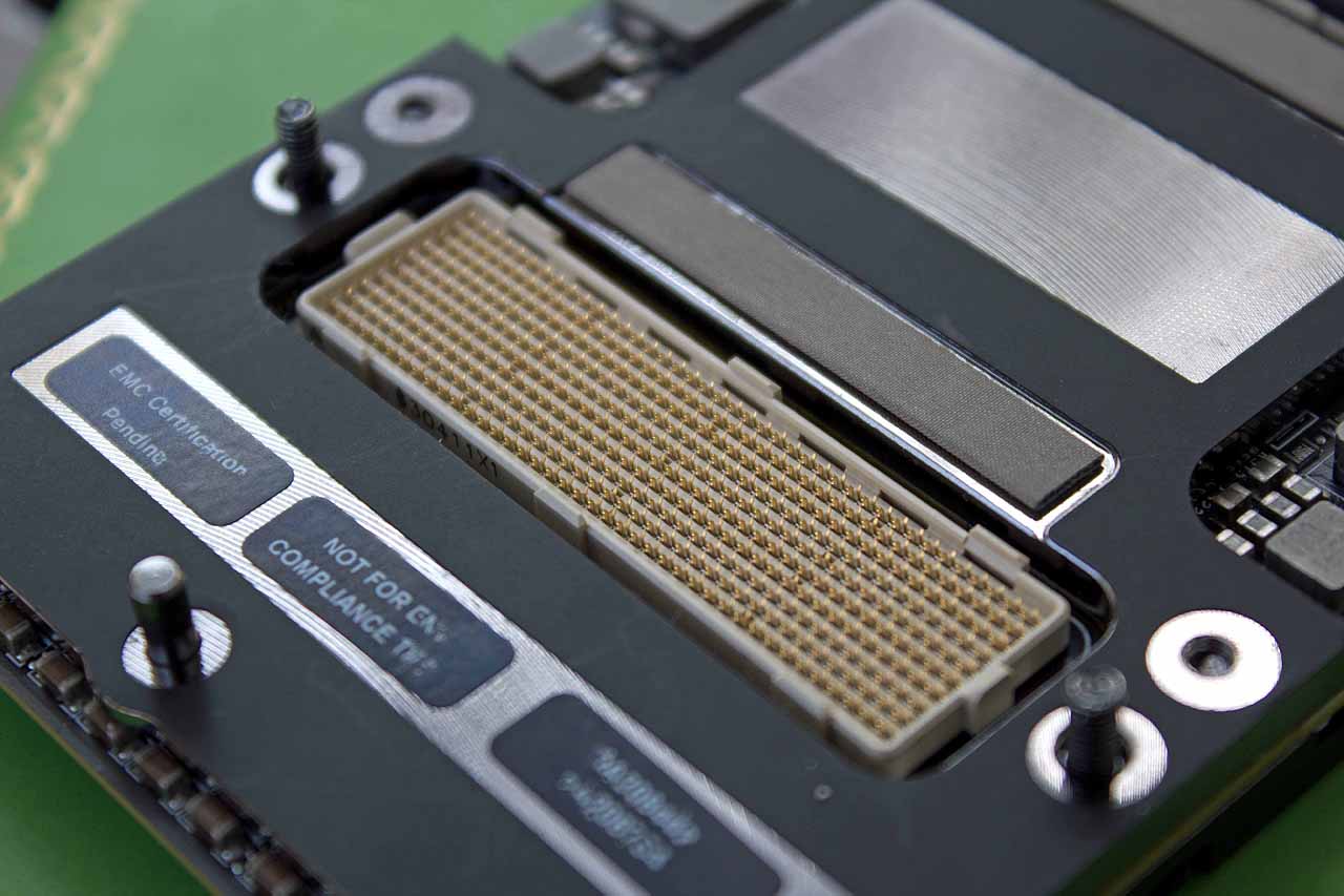
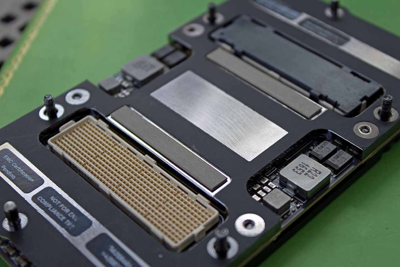
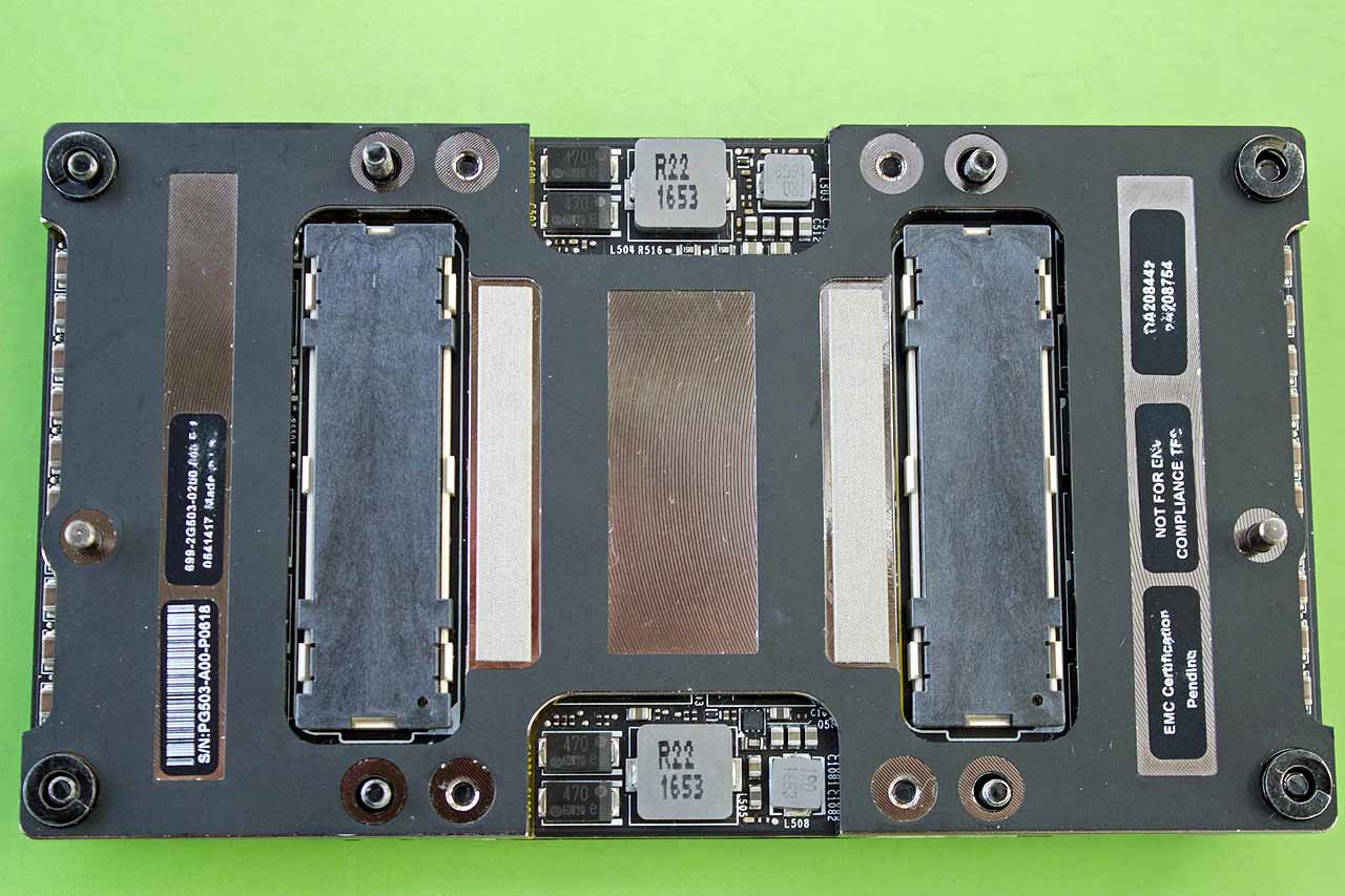
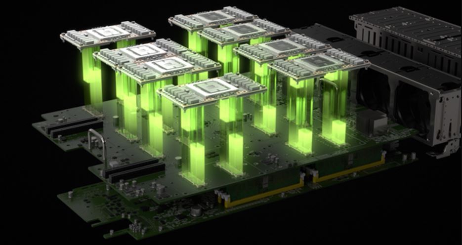
A hefty array of 16 inductors and voltage regulators line the edge of the card. The package pulls an average of 300W at a little below 1V, so over 300A flows into the die. Nvidia provides reference cooling designs, but most of its HPC customers opt for custom liquid cooling solutions, while many hyperscalers go with air cooling. The thermal solution attaches to the four silver-edged holes next to the die.
Get Tom's Hardware's best news and in-depth reviews, straight to your inbox.
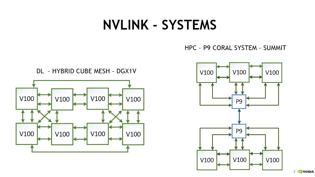
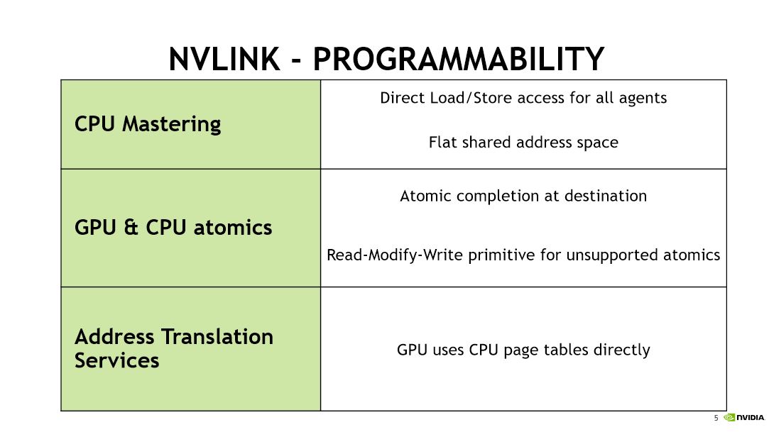
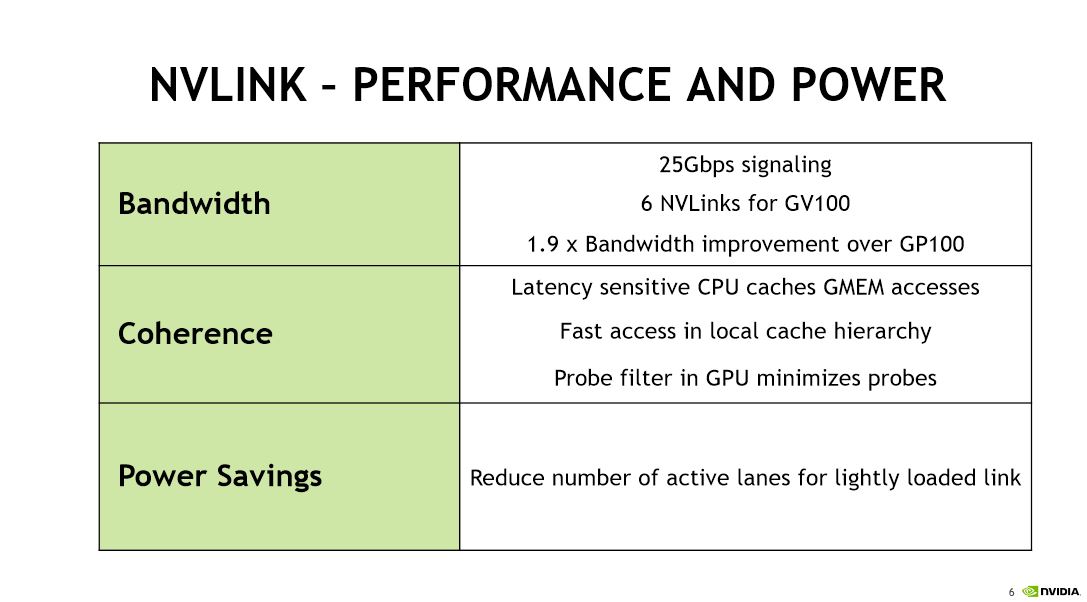
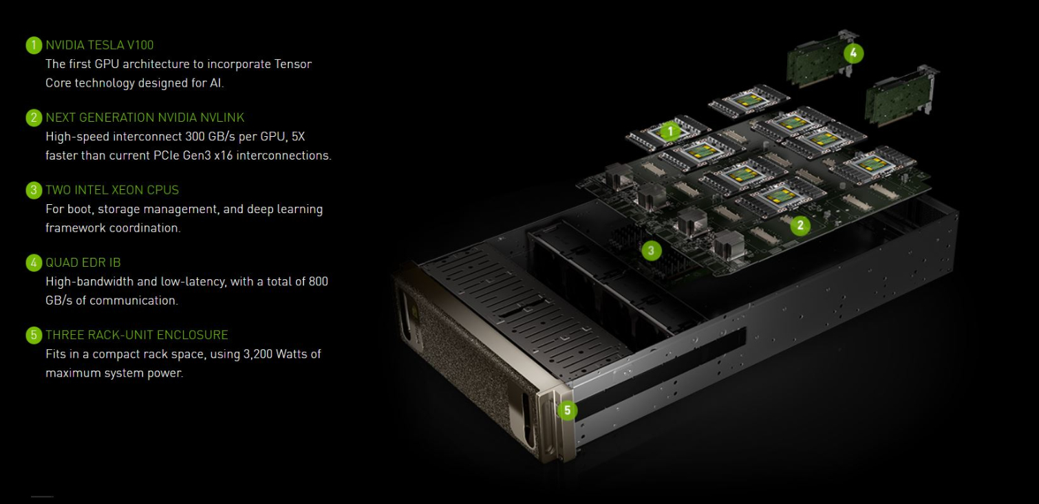
The Tesla V100-powered DGX-1 packs eight Volta GPUs crammed into a 3U chassis to deliver a whopping 960 TFLOPs of power from 40,960 CUDA cores. It also brings the addition of 5,120 Tensor cores (more coverage on that here), and six NVLink 2.0 connections increase throughput to 10X that of a standard PCIe connection (300GB/s). The DXG-1 draws up to 3,200W inside a single chassis, so effective cooling is a must.
Nvidia’s NVLink accommodates several system topologies, such as the hybrid cube mesh in the DGX-1 for machine learning applications and the HPC-specific P9 Coral System’s unique design. These topologies minimize peer-to-peer latency and provide multipathing capabilities.
Nvidia designed its proprietary NVLink protocol specifically for low latency and high-throughput peer-to-peer GPU communication. The company has considered opening up the NVLink protocol as a standard, but ultimately, Nvidia feels that could hinder development. Several large industry consortiums are developing competing open standards, such as CCIX and CAPI, but Nvidia believes NVLink is best suited for its specific use case.
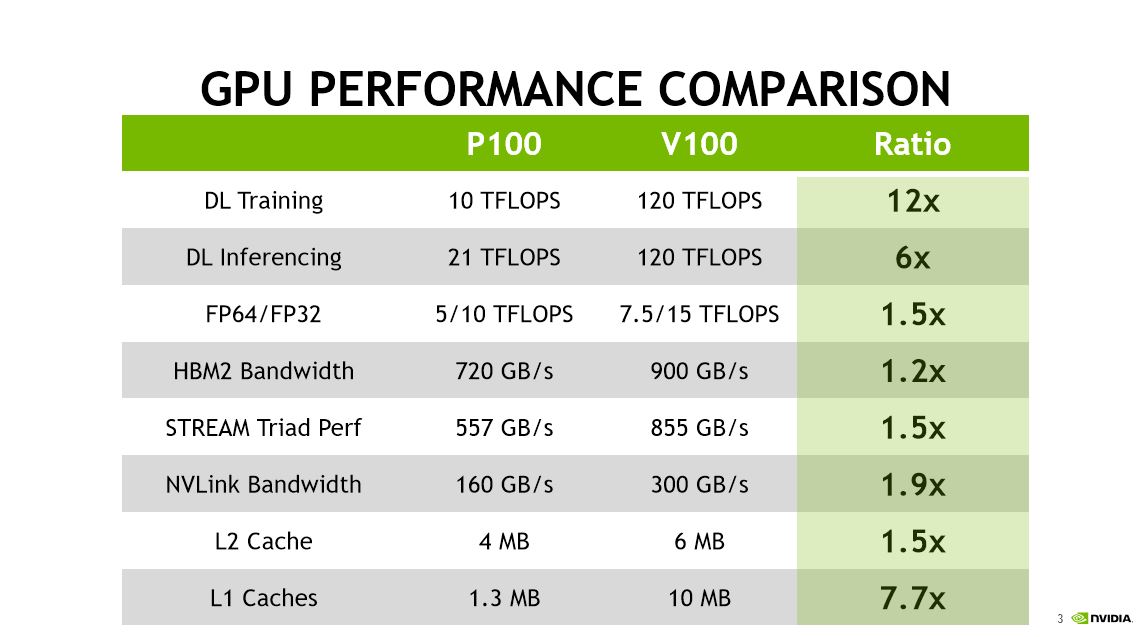
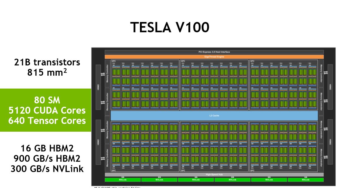
Nvidia claims impressive performance advantages over its previous-generation P100. Highlights include a 12x boost to training and a 6x boost for inferencing. Performance is fed, in part, by faster HBM2, L2, and L1 caches. Meanwhile, NVLink 2’s expanded bandwidth nearly doubles inter-GPU throughput.
The Volta GV100 SM
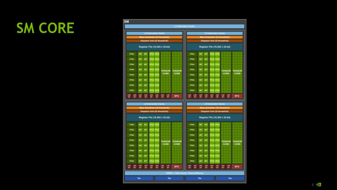
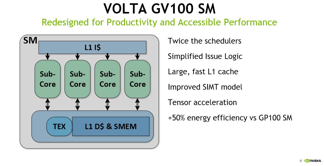
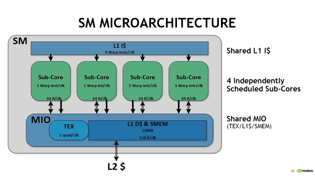
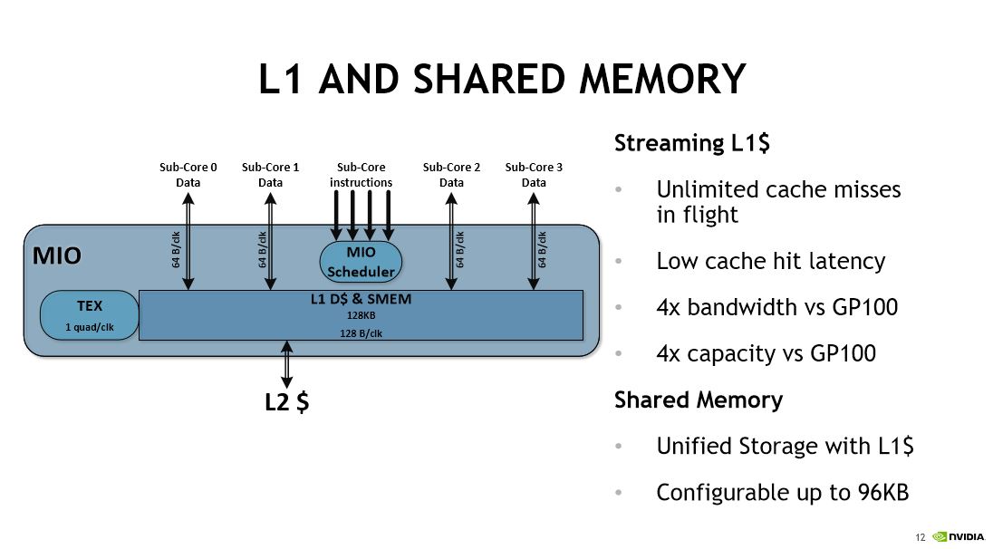
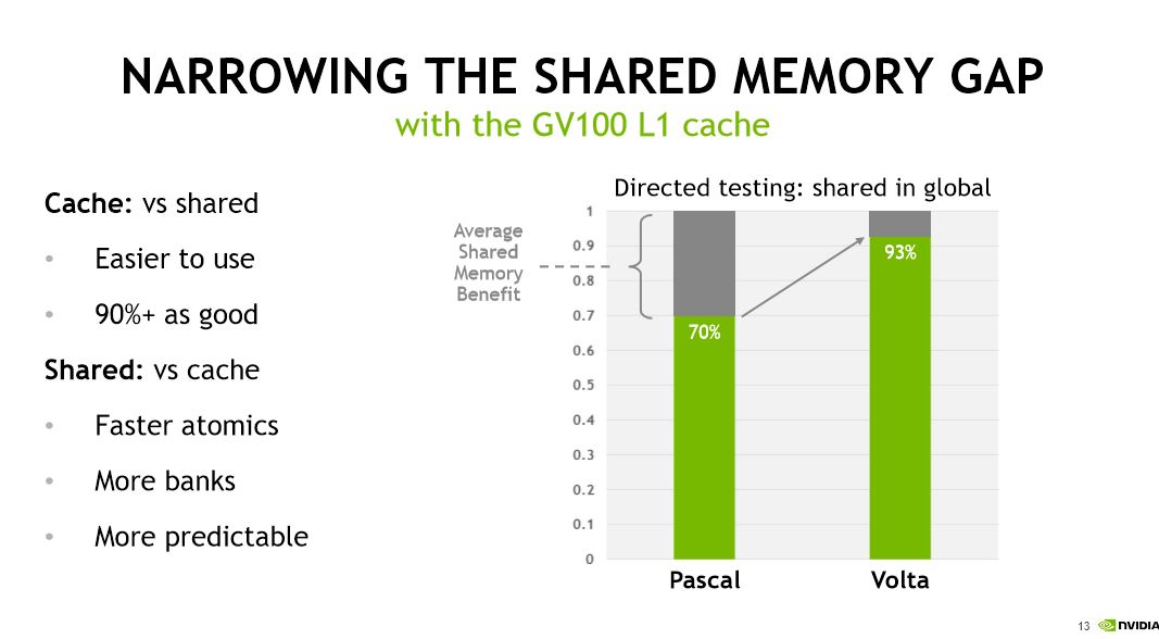
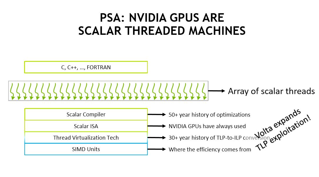
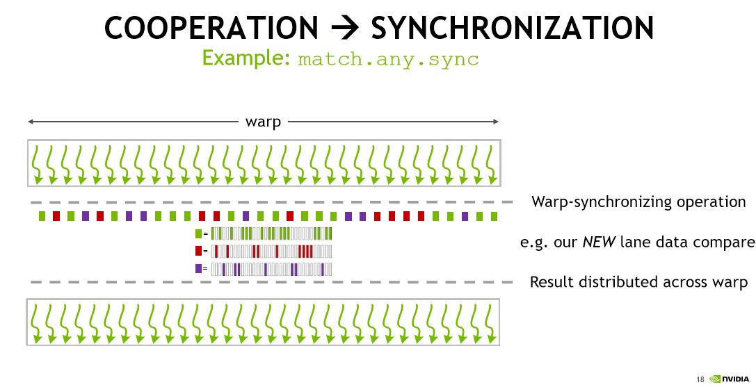
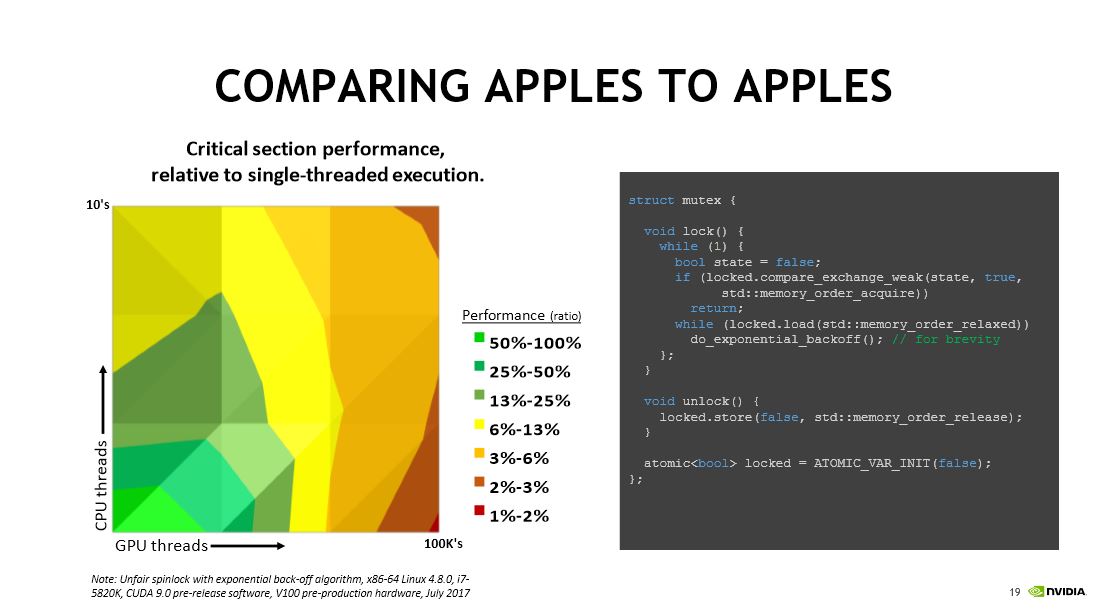
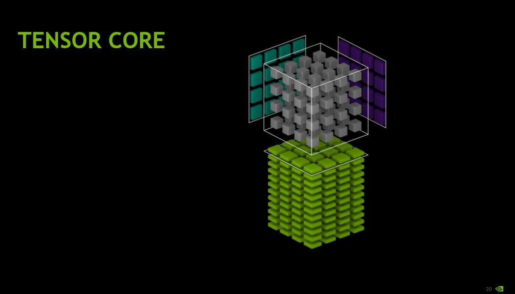
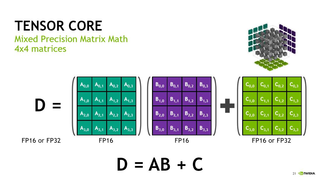
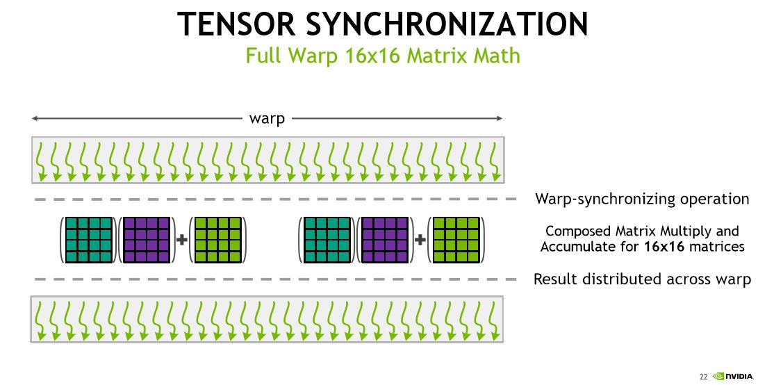
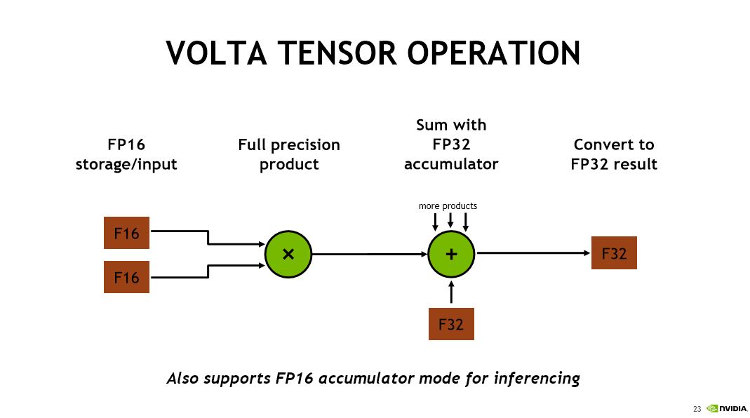
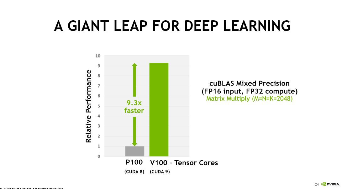
80 SMs, wielding a total of 5,120 CUDA cores and 640 Tensor cores, populate the die. Improvements include doubled warp schedulers, a large L1 instruction cache, and tensor acceleration. The shared L1 instruction cache feeds one warp instruction per clock to the independently scheduled sub-cores. Each sub-core processes one warp instruction per clock and feeds into the shared MIO unit. The MIO unit houses texture, shared L1 data cache, and shared memory.
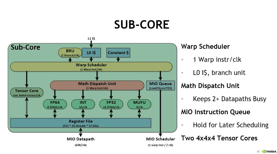
Each SM sub-core has its own L0 instruction cache and a dedicated branch unit. The warp scheduler feeds the math dispatch unit, sends MIO instructions to the MIO instruction queue for later scheduling, and feeds the two 4x4x4 Tensor cores (which are used specifically for deep learning).
The four sub-cores send instructions into the MIO scheduler. The 128KB L1 data cache provides 128 bytes of bandwidth per clock. Each sub-core has a 64 byte-per-clock connection to the L1 data cache. Nvidia noted that it designed the cache subsystem for superior data streaming performance; it offers four times the bandwidth and capacity compared to the GP100.
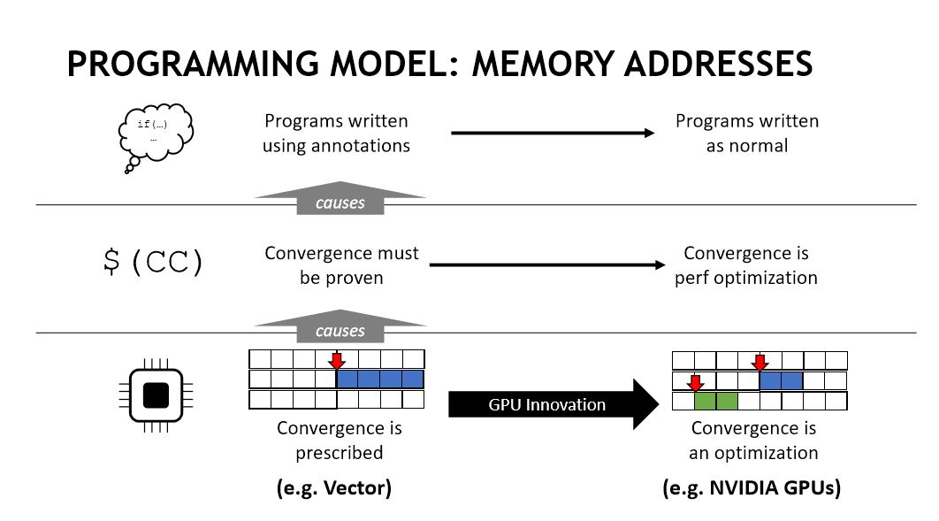
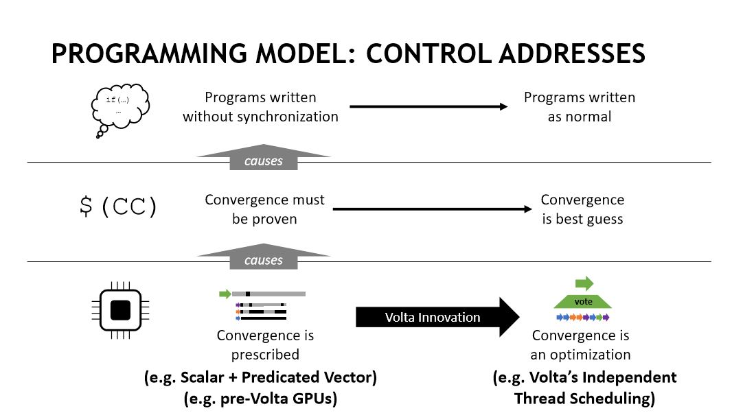
Nvidia also shared information on the Tesla V100’s independent thread scheduling, along with the mixed-precision FP16/FP32 Tensor cores for deep learning matrix arithmetic. The company has already released many of these details.
Nvidia is entrenched with several high-volume hyperscalers and high-volume customers, such as Facebook. Facebook developed its Big Basin platform, which is a custom system that leverages the V100 and Nvidia’s HGX reference board design. Facebook plans to release it to the Open Compute (OCP) project soon, so we can expect a wave of OEM and ODM systems to come to market with the new design. That’ll open more avenues for Nvidia to sell its data center GPUs, but Nvidia isn't commenting on when Volta-fueled GPUs will come to the desktop.

Paul Alcorn is the Editor-in-Chief for Tom's Hardware US. He also writes news and reviews on CPUs, storage, and enterprise hardware.
-
10tacle There had been rumors all year that Nvidia may do a Pascal refresh (GTX 20xx series) similar to what they did with Kepler (GTX 6xx --> GTX 7xx) prior to Volta. If they were going to do it, they'd have already done it by now.Reply
But 5,120 CUDA cores. Wow. Pascal's Titan X and 1080 Ti have 3,584. I just hope finally we'll have a true single GPU solution for 4K gaming at a solid 60FPS with the heaviest GPU hitting AAA titles (I'm looking at you, Dues Ex and Watchdogs 2). -
zippyzion I don't think NVidia needs to release Volta right now, and if they did it would be crazy expensive. They announced them quite a while ago and if they still have process issues that are causing low yields, anything they release would be a $1000+ card. Not to mention the cost and short supply of HMB2. My money is on a late Q1 or early Q2 next year launch for desktop graphics. Hopefully that gives them time to work out the kinks.Reply -
dg946f_lives It's been released and is selling very well. Jensen said as much during the webcast on 8/10.Reply -
bit_user Reply
It's already shipping.20099373 said:When would it be available ?
https://blogs.nvidia.com/blog/2017/08/07/ai-researchers-tesla-v100-nvail-isml/
But, if you have to ask, then you can't afford it. Like the P100, this surely will not be offered to gamers. You actually can get a GP100-based graphics card, but in the form of a Quadro workstation card. Read it and weep:
https://www.cnet.com/products/nvidia-quadro-gp100-graphics-card-quadro-gp100-16-gb/prices/
They haven't announced any consumer-level Volta GPUs.
-
TadashiTG @ZIPPYZION Volta as an architecture doesn't have "process issues". The V100 GPU core based on the Volta architecture has unavoidable "process issues" due to it's massive size.Reply
A desktop Volta GPU will definitely not be as big as the V100 and will most likely not use HMB2 either. So desktop parts will not cost a lot to manufacture should Nvidia choose to start manufacturing them.
Nvidia has no reason to release any new GPU line up because of the lack of competition at the high end as well as at the perf/watt metric. A refreshed Pascal might make sense in terms of driving a bit more sales I suppose, but I'm not sure about that, I mean they already released 1060 and 1080 with faster VRAM, that could have been saved for a Pascal refresh instead. -
bit_user Reply
You're comparing to the wrong GPU. The V100 should be compared to the P100 - not the GP102.20099506 said:But 5,120 CUDA cores. Wow. Pascal's Titan X and 1080 Ti have 3,584. I just hope finally we'll have a true single GPU solution for 4K gaming at a solid 60FPS with the heaviest GPU hitting AAA titles (I'm looking at you, Dues Ex and Watchdogs 2).
And the V100 is reportedly much more expensive than the P100 was. Based on that, I wouldn't expect the same ~43% increase in core count for the consumer GPUs. For gamers, the performance increase from Pascal to Volta will actually be smaller than Maxwell -> Pascal. If you already have a 1080 Ti, then you'll probably skip the 1180 Ti. But if you have a 1070, 1080, or a 980 Ti (like me) then 1180 Ti should be pretty interesting.
-
bit_user BTW, 3.2 kW in 3U.Reply
Wow.
I would not like to be around one of the air-cooled units at full bore. I wonder how much power the fans, themselves, actually burn. -
Martell1977 So they went from 16nm process to a 12nm process? That's not much of a change for a GPU. I would have thought they would wait like AMD for the 7nm process and use the 16nm for a couple generations. SHould be interesting to learn exactly what was gained by changing it.Reply -
d0x360 Nvidia would be wise to release a consumer version with at least 12 gigs of HBM2. People are under the impression that amd has no answer for this but they do. The Vega was delayed so much because of issues with HBM2 yields. It's still not sorted as this article obviously states BUT it is the best way to go.Reply
Next year and is going to launch something big that's essentially an optimized Vega that uses less power but delivers far more performance. People also forget amds architecture allows them to do more per clock cycle than nvidia.
That's nvidias mistake and they are making it again here. They keep chasing higher clocks to brute Force rendering. It's managed to beat amd because their architecture wasn't up to the task but that has changed
nVidia needs to be ready and it's likely they are already building consumer versions and running tests then making changes. Unfortunately for them they can't change the way it renders as far as the full path goes. Their architecture is like Intel and amd has once again found a way to be the best. They just need a few more months to refine what is already an excellent design for both the CPU and GPU market.
Brute Force only gets you so far. Finesse is not in their playbook at all but it's the basis for everything and is setting up.
