Epyc AMD Milan-X Delidding Reveals Intricate 3D-Stacked Design (Updated)
Presentation slide deck diagrams aren't like the real thing.

Update 4/21/2022 8:20am PT: Wassick's further analysis has revealed new details about the design, including a silicon cap that is placed on top of the SRAM and silicon shims. We have amended the story accordingly:
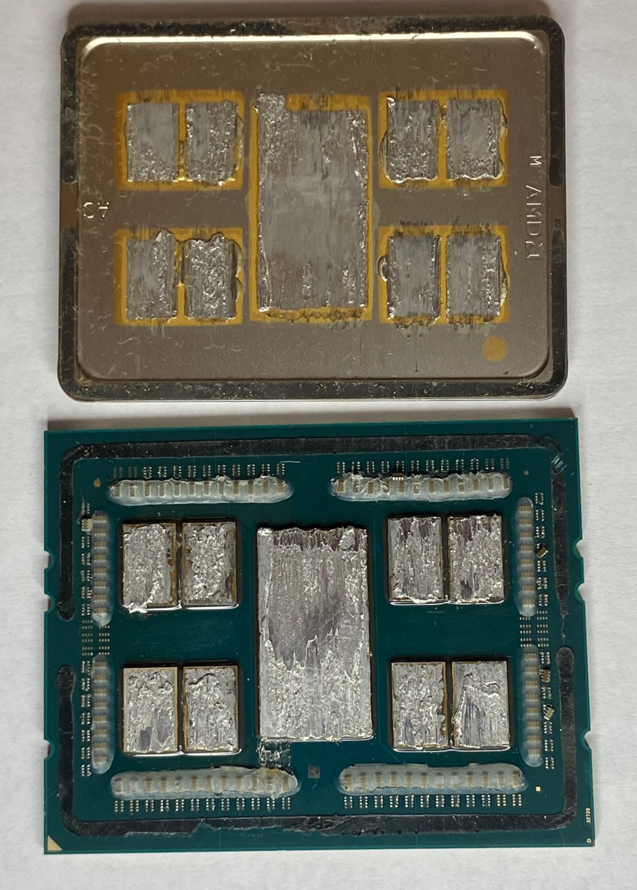
One of AMD's new generation Epyc Milan X processors has been delidded by Tom Wassick, revealing an intricate design that includes an extra layer of silicon on top of the stacked SRAM and silicon shims. This same design is present on the Ryzen 7 5800X3D chips that have proven to be the best CPUs for gaming.
Wassick, a semiconductor packaging engineering professional, takes his inquisitiveness into computer chips to a deeper level than most. His deconstruction of a new AMD server processor started with delidding. As Wassick wasn't undertaking this process to change the Thermal Interface Material (TIM) or heatspreader for (extreme) overclocking purposes, he wasn't too upset about trashing a few capacitors in the process.
Literally under the cover now (trashed a few capacitors...): pic.twitter.com/Agq7mwVPRnApril 18, 2022
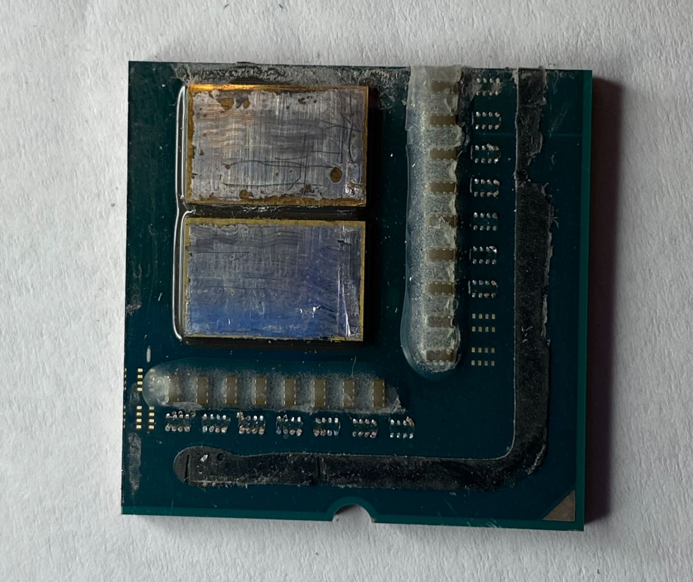
After the above initial reveal, Wassick was intrigued and went further, scraping off the TIM from where it had oozed. However, there were no boundaries in the construction to be seen and no visibly separate silicon shims in the layout.
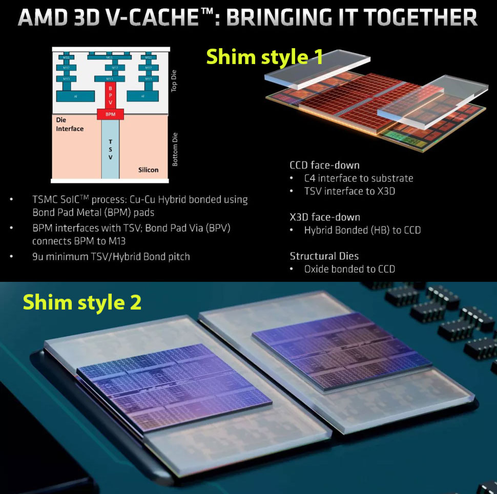
Wassick's further work implied that the Milan-X chip relied on "a monolithic piece within which the active SRAM is embedded," meaning the SRAM portion of this single upper die appeared to reside in the middle and be flanked by 'blank' areas of silicon. This is quite different from the structure AMD had outlined in previous illustrations provided by the company (see below).
Wassick explained that he also checked Milan-X's structure, with its lack of silicon shims and monolithic top-die design, with an IR camera. The last entry in Wassick's Twitter thread about his Milan-X surgery was to tell followers that he was going to follow up the work done so far by examining cross-section cuts of the die.

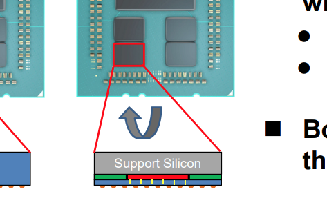
After further examination of the cross-section data, Wassick found that the design incorporates five pieces of silicon, instead of the four shown in most of AMD's diagrams. However, the below image from AMD's ISSCC presentation is accurate:
Get Tom's Hardware's best news and in-depth reviews, straight to your inbox.

Notably, this image is much different than AMD's other publicly-shared imagery, but it certainly isn't uncommon for chip illustrations to not follow the actual design very closely. However, Wassick's detective work has determined that this in fact the actual layout.
As you can see in the above diagram, the blue die (the CCD) has an SRAM die (red block) placed on top. The SRAM is flanked by the silicon shim (green - more detail below), all of which have yet another slice of support silicon (grey) on top. The blue die mates with the PCB on the chip package, and AMD applies indium solder to the top of the upward-facing support silicon. This then mates with the integrated heat spreader (IHS).
Here we are: a top die without seams indicating it's a monolithic piece, within which the active SRAM is "embedded": pic.twitter.com/a7T2Nggh8iApril 18, 2022
In the end, the silicon shims are basically used as structural thermal pads to ensure good contact between the stacked structure and the IHS. Thus, all the die components are close enough in height for a few dabs of indium to do the job of passing heat to the IHS that sits atop the stacked dies.
3D v-Cache Accelerates HPC Tasks by up to 50%
AMD Epyc Milan-X only started shipping to customers last month and it is an interesting and important processor as it brings the same 3D V-Cache technology, as featured in the Ryzen 7 5800X3D, to servers.
While on the PC/consumer side of things we only see significant benefits to 3D V-Cache in gaming, AMD says some High Performance Computing (HPC) workloads are even more receptive to the large (512MB) TSV-connected fast cache. Milan-X can "deliver up to a 50% performance increase across technical computing workloads like computational fluid dynamics, EDA, and any sort of advanced physics modeling," said AMD.

Mark Tyson is a news editor at Tom's Hardware. He enjoys covering the full breadth of PC tech; from business and semiconductor design to products approaching the edge of reason.
-
InvalidError I'd imagine making a U-shaped shim that fits snugly around the cache chip would be a quite substantial manufacturing challenge.Reply -
digitalgriffin ReplyInvalidError said:I'd imagine making a U-shaped shim that fits snugly around the cache chip would be a quite substantial manufacturing challenge.
I was thinking the same thing. To be honest I'm surprised the cache wasn't on the bottom of chip on the 5800X3D. The side with the most energy dissipation/density should be side up to the heat sink. -
InvalidError Reply
Putting the cache at the bottom would cause its own lot of problems with passing 100+A through the extra layer, along with all of the high-speed signals. Adding it on top has much fewer potential points of failure at the expense of slightly worse thermal performance.digitalgriffin said:I was thinking the same thing. To be honest I'm surprised the cache wasn't on the bottom of chip on the 5800X3D. The side with the most energy dissipation/density should be side up to the heat sink.
One way to make the top slab look monolithic at a glance but actually be a separate piece to save 7nm silicon would be to etch or machine a pocket in the slab for the cache die. -
escksu Replydigitalgriffin said:I was thinking the same thing. To be honest I'm surprised the cache wasn't on the bottom of chip on the 5800X3D. The side with the most energy dissipation/density should be side up to the heat sink.
AFAIK, Zen3 chiplets have their circuits facing "up" instead of "down" (not a flipchip design). these chiplets are using TSV to connect the chiplets to the substrate. So, what this means is that those contact bumps on the chiplets are at the bottom.
So, it is not possible to put the cache at the bottom. AMD is trying to minimise changes to the die, so the easiest and most cost effective way is to simply place the cache die on top of the chiplet. -
InvalidError Reply
AMD's description of the cache chip attachment process contradicts that: it says the back of the CCDs needs to be etched away to expose the TSVs to which the cache chips will be attached, which means the cache chips are the ones attached to the back of the CCDs through the CCDs' TSVs which are still present but hidden and not doing anything on non-3D chiplets.escksu said:AFAIK, Zen3 chiplets have their circuits facing "up" instead of "down" (not a flipchip design). these chiplets are using TSV to connect the chiplets to the substrate.
