GlobalFoundries Infuses 22FDX Platform With ST-MRAM Memory
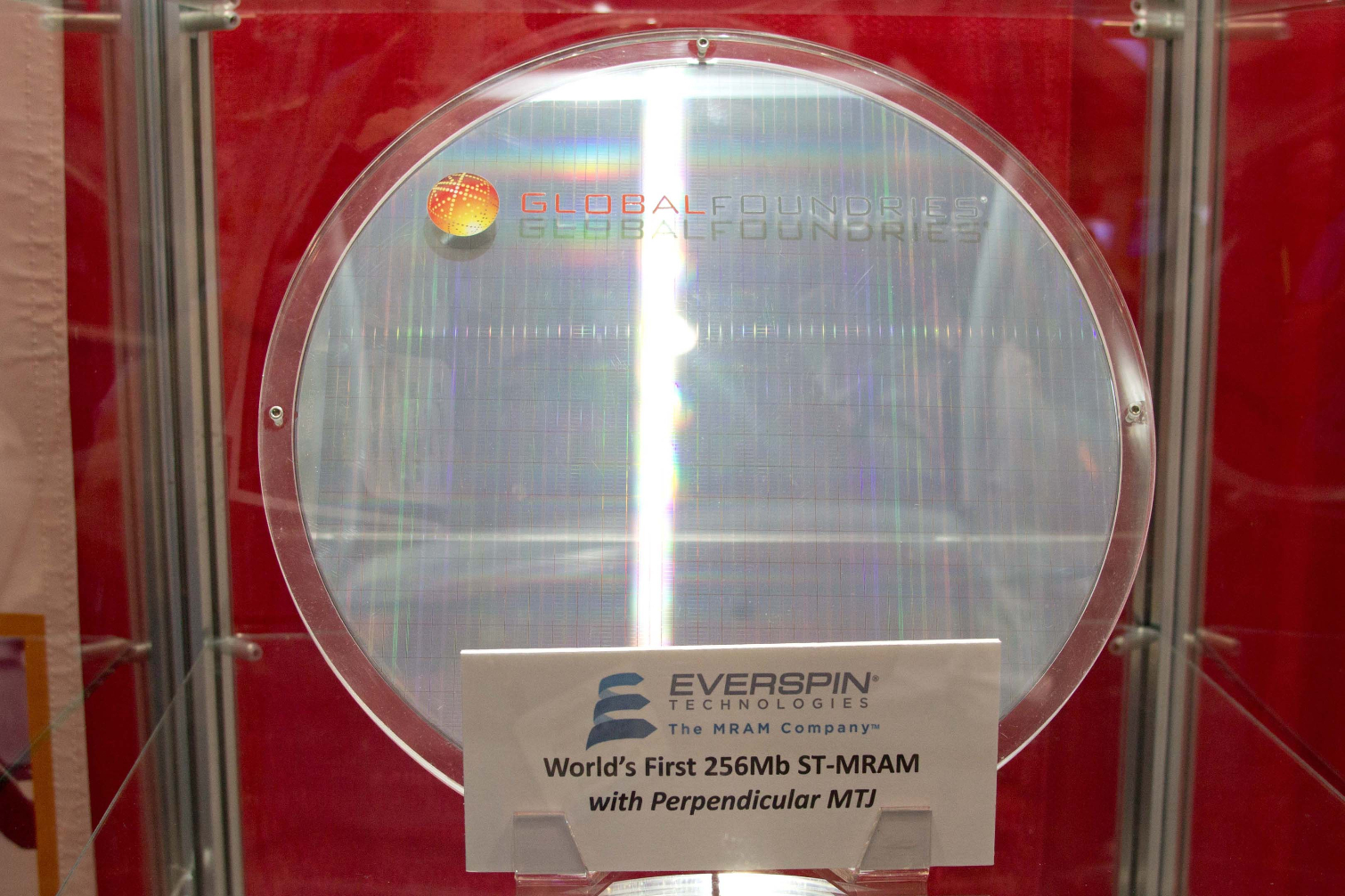
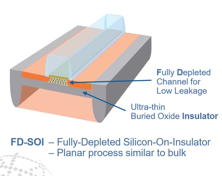
GlobalFoundries announced that it is producing embedded non-volatile Magnetoresistive RAM (ST-MRAM) for use in its 22FDX platform. GlobalFoundries' 22FDX platform is the first 22nm fully-depleted silicon-on-insulator (FD-SOI) technology, and the addition of its eMRAM (its marketing term for ST-MRAM) will give it a revolutionary new tool for SoCs and MCUs.
Most MRAM development initiatives have languished in the research lab. Several industry heavyweights, such as IBM, Toshiba, and Samsung, are working on MRAM but have yet to offer products. GlobalFoundries is licensing its ST-MRAM technology from Everspin, which is the only company that has actually productized the speedy memory. Everspin and Global Foundries have jointly designed and produced ST-MRAM devices on 300nm CMOS wafers with a 48nm lithography since 2014, and the companies have declared they have plans to move to 28nm in the near future.
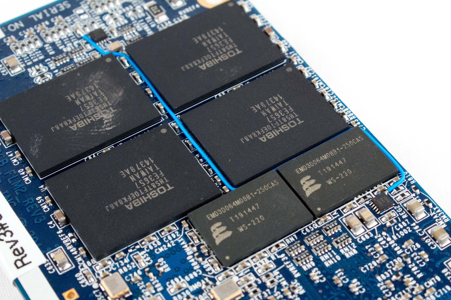
MRAM can replace SRAM/eDRAM in some embedded chip applications, and it can also be used as standalone storage-class memory. Unlike other emerging memories, ST-MRAM isn't a futuristic technology; we recently tested the Mangstor MX6300, which is one of the first enterprise-class SSDs to employ the promising new medium as a buffer. RAID controllers have also used MRAM for several years.
Article continues below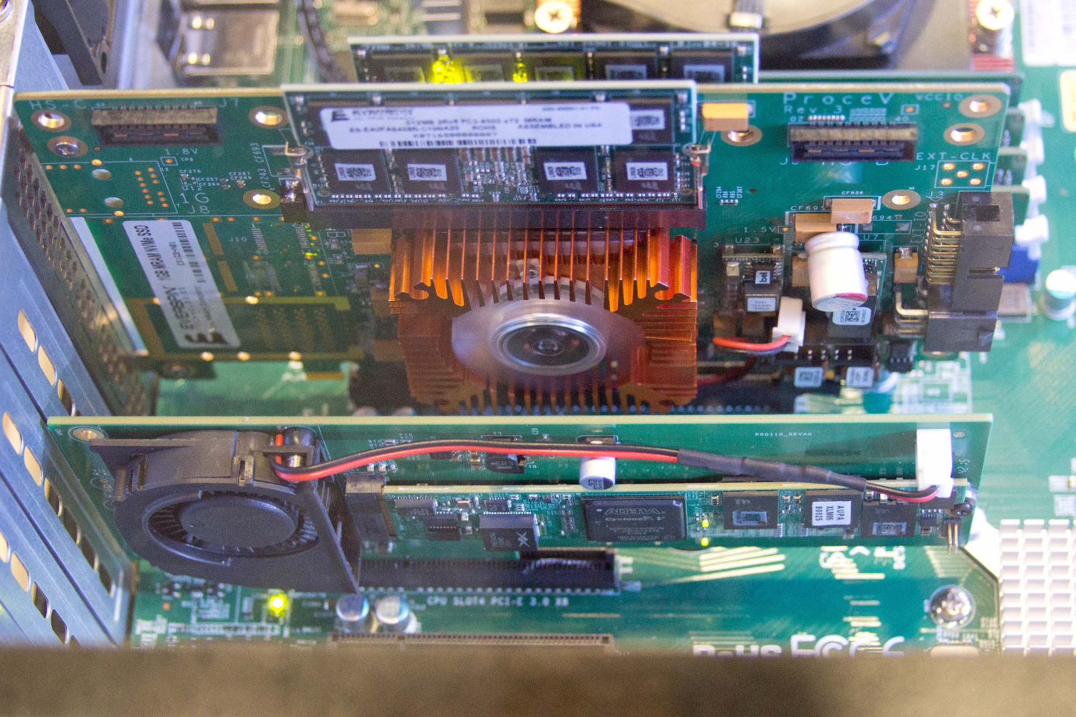
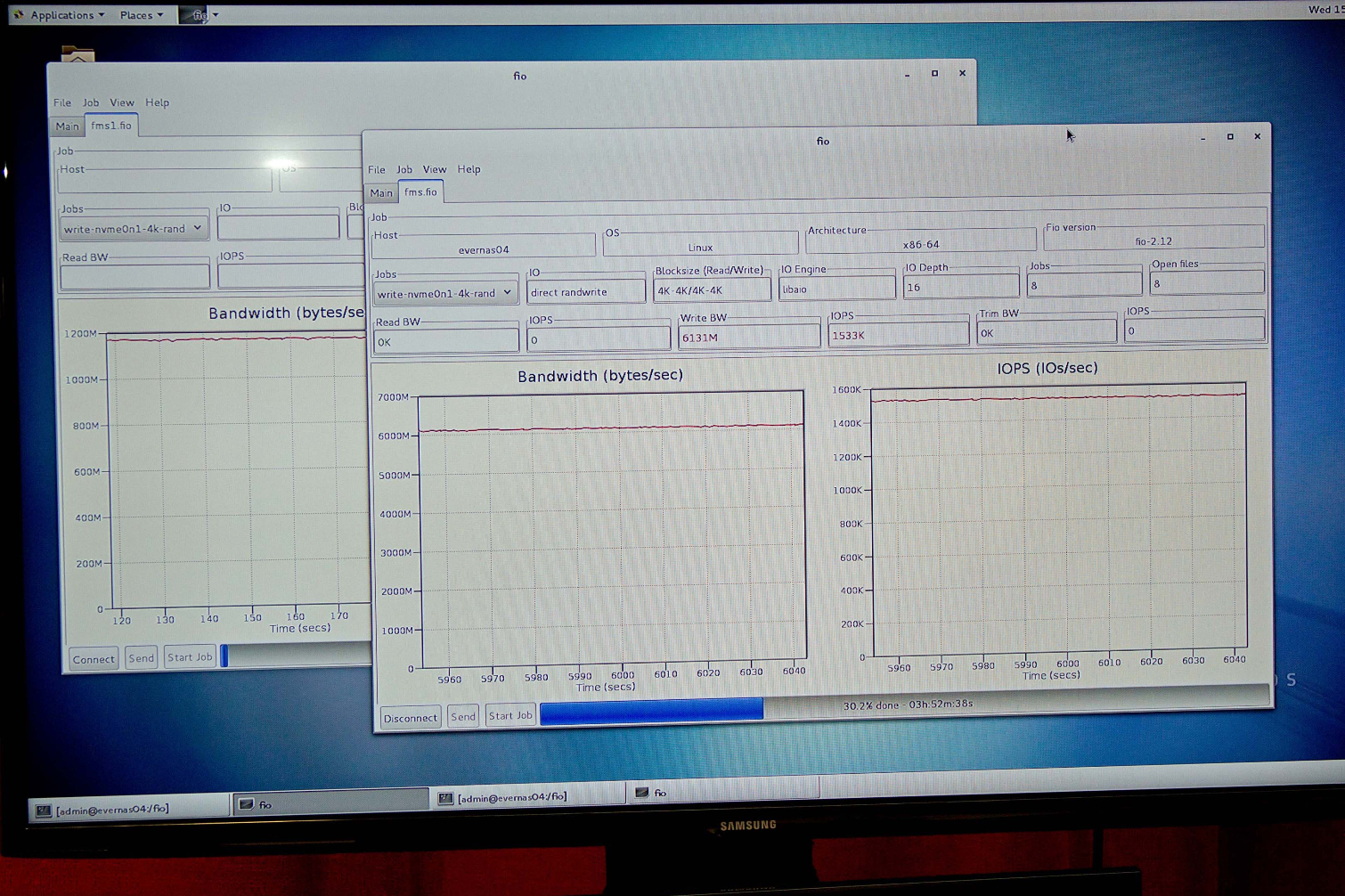
At the recent Flash Memory Summit, Aupera treated us to a working demo of its M.2 MRAM SSD on a carrier card (foreground) pushing out 1.5 million 4K random writes, or more than 6GB/s of sustained random throughput. MRAM currently has very limited capacity; the M.2 MRAM SSD featured only 128MB of capacity. MRAM will require more density before it can compete with other storage-class memories, such as 3D XPoint or carbon nanotube-based memories. Everspin and GlobalFoundries are banking on increased density through lithography shrinks.
Of course, the real interesting bits are just how MRAM works, and how it can revolutionize processor design.
The Works
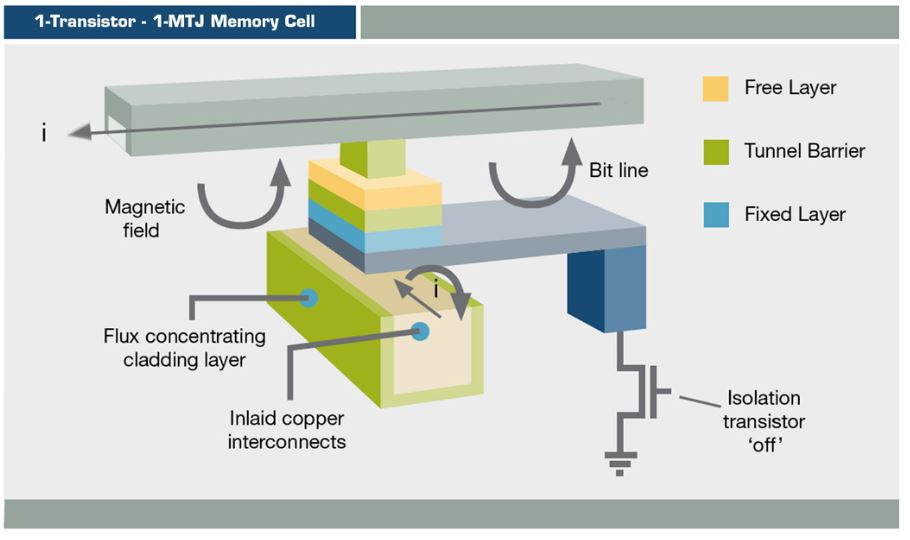
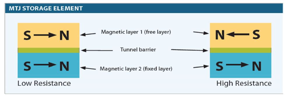
MRAM comes in many flavors, but Everspin uses Spin-Torque (ST-MRAM) technology. MRAM stores data magnetically, which is in stark contrast to electron-based data storage techniques. MRAM retains all stored data when the device loses power (which means it is a persistent non-volatile storage medium). A perpendicular magnetic tunnel junction (pMJT), which HDD vendors use in read heads, serves as the memory cell. It uses standard CMOS transistors. The design consists of two ferromagnetic plates with an insulating dielectric layer between them. One plate is set to a known polarity (fixed layer), and the other plate's polarity can be changed (free layer). If both plates have matching polarity, the cell will be in a low-resistance state (1), and if they have different polarity, the cell will be in a high-resistance state (0). The device measures the resulting electrical resistance to determine if the cell holds a "1" or "0." The cell does not have to be erased before it is rewritten, which simplifies management and increases performance.
MRAM is purportedly less expensive to produce than DRAM, but as with any emerging memory technology, density is the key to economical production. MRAM is faster than DRAM, and current products communicate with the DDR3 protocol. GlobalFoundries and Everspin are currently producing 256Mb devices (48nm) and have 1Gb devices that leverage the DDR4 protocol (28nm) in the pipeline. The companies also have a clear road map to denser climes (sub-20nm) in the future.
Get Tom's Hardware's best news and in-depth reviews, straight to your inbox.
MRAM has almost unlimited endurance for most practical applications, and Everspin has tested it to 10^10 cycles (tens of millions more times endurant than NAND). Heat is almost a non-issue; eMRAM can retain data through 260C solder reflow. MRAM is touted as a replacement for NOR and SRAM in embedded chip applications, and its persistent state reduces power consumption because it doesn't require cell refresh power, has virtually no leakage, and requires up to a 1,000x less energy during write operations. MRAM's persistence also eliminates rebuilding the memory structure when a device resumes from sleep, which would have a transformative effect on the way processors manage the cache.
GlobalFoundries positions its leading edge products for IoT and automotive SoCs and MCUs. Most processors dedicate between 50-80% of the die to memory, and SRAM typically employs ~6 transistors, whereas MRAM only uses one. MRAM's increased density and design simplicity are tantalizing prospects for semiconductor vendors.
Will ST-MRAM Come To 12FDX?
GlobalFoundries also unveiled its 12FDX 12nm FD-SOI technology last week, and it is a logical assumption that we can expect the company to include eMRAM technology as it matures. The 12nm FD-SOI promises to be competitive against FinFET designs; GlobalFoundries designed it to offer the performance of 10nm FinFET at a lower cost than 16nm FinFET. The company contends that its 12FDX platform offers a 15% boost over existing FinFET and reduces power consumption by 50%.
12FDX sets a new standard for system integration, providing an optimized platform for combining radio frequency (RF), analog, embedded memory, and advanced logic onto a single chip. The technology also provides the industry’s widest range of dynamic voltage scaling and unmatched design flexibility via software-controlled transistors—capable of delivering peak performance when and where it is needed, while balancing static and dynamic power for the ultimate in energy efficiency.
GlobalFoundries and Everspin expect eMRAM to sample for prototyping in 2017, and mass production is slated for 2018. The 12nm 12FDX FD-SOI platform should go into production in GlobalFoundries' Fab 1 in Dresden with initial tape-outs predicted for 2019.

Paul Alcorn is the Editor-in-Chief for Tom's Hardware US. He also writes news and reviews on CPUs, storage, and enterprise hardware.
-
blazorthon MRAM has long (like decades) been a viable memory technology. The biggest problem with it is just that most companies that work on MRAM don't work together, so it tends to not go far. It has been used in a lot of small embedded designs, especially those where non-volatility and high tolerance for heat and radiation are important. Mainstream usage has been low despite it's many advantages. It can be made far denser than SRAM while being similarly fast, non-volatile, having lower power consumption, and not being too difficult to produce, but like most memory technologies that didn't quickly hit mainstream, it never really got enough fab allocation. The companies don't really like spending the big money on products that they aren't 100% certain they can sell, so they mostly just go on producing products they're already selling, like DRAM.Reply -
aldaia Reply18620513 said:I'm not sure this is going to compete against Intel's 3D XPoint very well though.
MRAM and 3D XPoint are not competing products, they fit in diferent segments.
MRAM is fater than DRAM, some say its as fast as SRAM, 3D XPoint is 5-8 times slower than DRAM
3D XPoint is about 1000 times more durable than NAND, while MRAM is "tens of millions more times endurant than NAND"
MRAM has similar density to DRAM, while 3D XPoint is expected to have packing density 8-10 times greater than DRAM
Short term I see MRAM as a replacement for SRAM and DRAM, while 3D XPoint can be a replacement for NAND
Long term, if MRAM can be made more dense and 3D XPoint can be made faster, then , yes i can see them competing. But I bet more on a new futuristic technology that replaces them both. -
blazorthon Reply18619897 said:I'm not sure I get it... how sensitive are these MRAM's to external magnetic fields?
https://www.everspin.com/frequently-asked-questions
So, this got me going. First, I looked up a data sheet of one of their current products:
EST00352_MR4A16B_Datasheet_Rev11.4 031116.pdf
Scrolling down, the max magnetic field strength is listed as 8000A/m. I fond a website saying that a strong neodynium magnet has a maximum field strength of about 12,000 Oe. Converting units gives 8000A/m = about 100Oe. So, like with hard drives, don't stick strong magnets near this stuff. A fridge magnet is probably safe, but any decent magnet should be kept away.
Other MRAMs products might have more or less shielding. I'm not going to look through all of their data sheets to find an average or anything, so take these results with a grain of salt. I can't say whether the MRAM made on the newer process in the article will be significantly different regarding sensitivity to external magnetic fields when compared to the product from the data sheet I found.
Other links I used:
http://www.wikihow.com/Determine-the-Strength-of-Magnets
http://www.translatorscafe.com/cafe/units-converter/magnetic-field-strength/oersted-%5Boe%5D-to-ampere-turn-per-meter-%5Bat/m%5D/ -
Kewlx25 Reply18619897 said:I'm not sure I get it... how sensitive are these MRAM's to external magnetic fields?
Electrons from adjacent atoms are probably exerting magnitudes more electro-magnetic stress on the MRAM than an external magnetic field.
I would love for someone with a physics background to give a more definitive answer. -
summakor MRAM is hard to do because it's not electrical. SRAM, DRAM and Flash are fundamentally all based on silicon transistors with more or less capacitance between the elements, depending on how fast you want it to be, how much power you're willing to use and how long you want the data and the device to endure. MRAM is truly different. Half a century of breakneck progress on Si transistors doesn't help with the physics of tiny magnets. The parent industry of MRAM is hard drive read heads, an industry that's been losing market share, R&D investment and staff for two decades. Magnets - how do they work??Reply
