Intel Demonstrates Industry’s First Co-Packaged Switch With 1.6Tbps Silicon Photonics
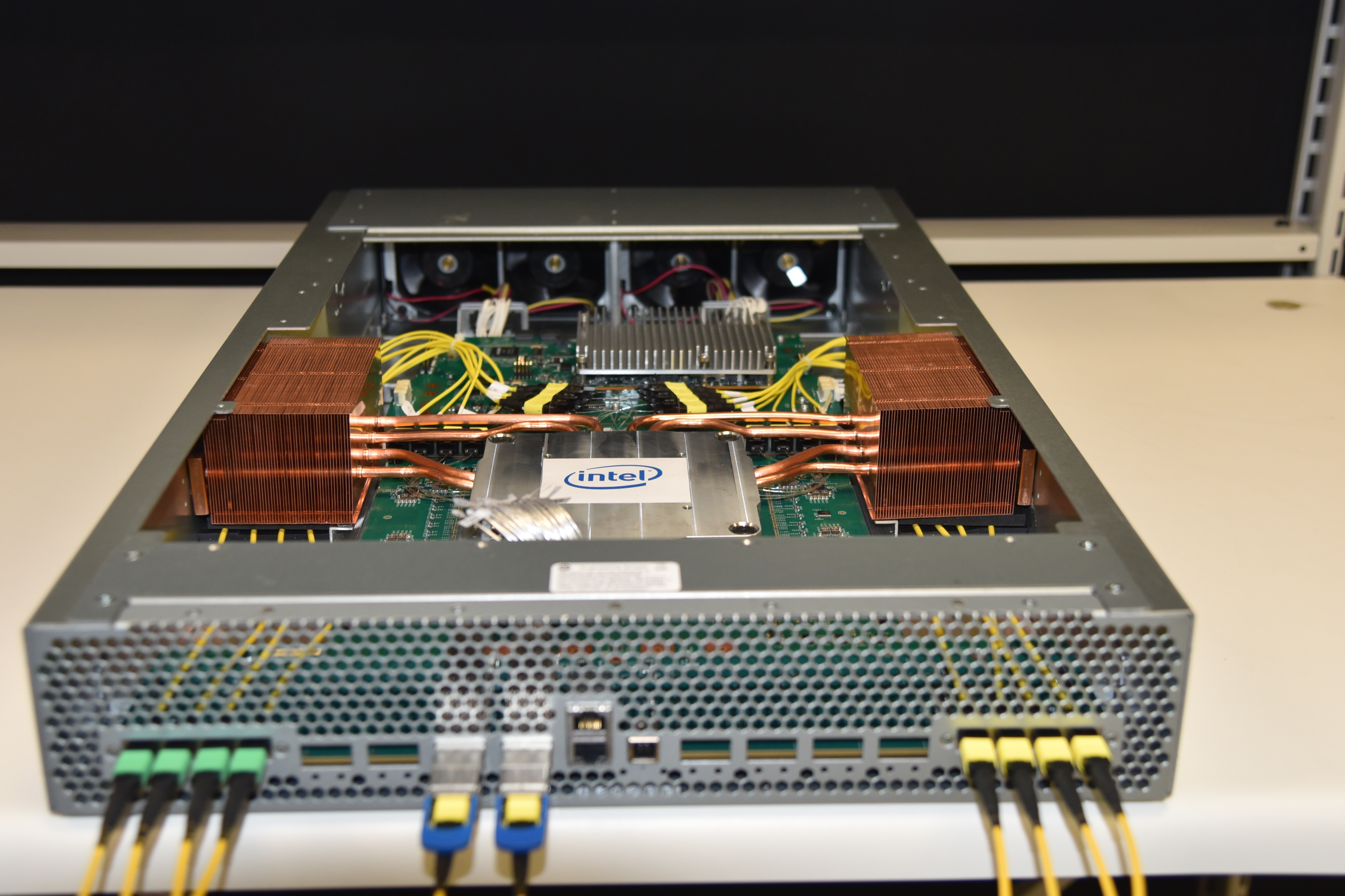
Intel has demonstrated the industry's first integrated switch package with silicon photonics.
Intel today announced a new breakthrough for co-packaged silicon photonics optics Ethernet switches. The company has integrated next-generation 1.6Tbps silicon photonics engines with the 12.8Tbps programmable Tofino 2 Ethernet switch Intel acquired from Barefoot Networks last year.
With the emergence of hyperscale cloud data centers, demand for data bandwidth has become practically limitless. To provide cost-effective interconnect solutions, Intel has been on a path to increase the bandwidth of its silicon photonics, which has been available in a 100Gbps pluggable optics form factor since 2016. Last year, Intel announced it would start production of 200Gbps and 400Gbps in the first half of 2020 and has used the present demonstration to reiterate this. Intel disclosed it has shipped over 3 million 100G pluggable transceivers to date.
Simultaneously, Intel has also been looking to further integrate its silicon photonics technology. In the common pluggable topics (QSFP28) form factor, the optics are installed in the switch faceplate, which in turn is connected to switch SerDes ports using an electrical trace. However, Intel says that as bandwidth grows, connecting the pluggable optics to the SerDes becomes more complex and consumes more power.
Article continues below 
This is where co-packaged optics come in, which Intel said is an industry-first. In this methodology, the optical port is placed near the switch, within the same package. This reduces power and enables the continued scalability of switch bandwidth, Intel described. The integrated switch package “features a combination of co-packaged optical ports and copper ports supporting front-plate cages for optical modules or copper cables.”
It appears Intel used a future version of its silicon photonics technology, as it uses 1.6Tbps silicon photonics engines from Intel’s Silicon Photonics Product Division. The engines are “realized as 4 ports of 400GBase-DR4 interfaces”, and are designed and manufactured in the Intel silicon photonics platform, according to Intel. For comparison, the current 100Gbps silicon photonics uses four 25Gbps ports. In silicon photonics, the laser is integrated on-chip and manufactured on Intel's 300mm wafer CMOS technology.

For the switch, Intel has leveraged the 12.8Tbps Tofino 2 switch ASIC from Barefoot Networks. The Tofino 2 switch consists of a multi-die package that makes the co-packaging easier as well as upgrading the SerDes. This is reminiscent of Intel’s chiplet approach with its 10nm Agilex FPGA.
Intel notes that the technology is “ready” and represent a first step towards optical I/O with silicon photonics:
Get Tom's Hardware's best news and in-depth reviews, straight to your inbox.
“Our co-packaged optics demonstration is the first step to making optical I/O with silicon photonics a reality”, said Hong Hou, Intel corporate vice president and general manager of the Silicon Photonics Products Division. “We share the industry belief that co-packaged optics offers power and density advantages for switches at 25 Tbps and higher, and ultimately is a necessary and enabling technology for bandwidth scalability in future networks. The timing of this demonstration shows the technology is ready to support our customers’ requirements.”
Intel acquired Barefoot Networks last year. We speculated at the time that it would integrate both technologies and was a major reason for the acquisition. Today’s announcement of Intel’s integrated switch package seems to confirm this. Intel said it is currently demonstrating the technology to customers, but did not provide a timeline for a commercial release.