Kioxia Says 3D XPoint ‘Isn’t the Future’

Kioxia claims that (3D) Storage-Class Memory (SCM), like 3D XPoint, isn’t the future and has no long-term propects. As reported by AnandTech, that was set forth by the company at the recent IEDM conference, where the company instead promoted its BiCS flash and XL-Flash technologies. The reason would be poor cost per bit scaling as the number of layers increases.
In the latter half of last decade, the flash industry moved to 3D NAND. Compared to conventional NAND, the size of the cell was reduced, but this was more than compensated by stacking layers vertically, for instance featuring 96 layers in Kioxia’s latest 3D NAND.
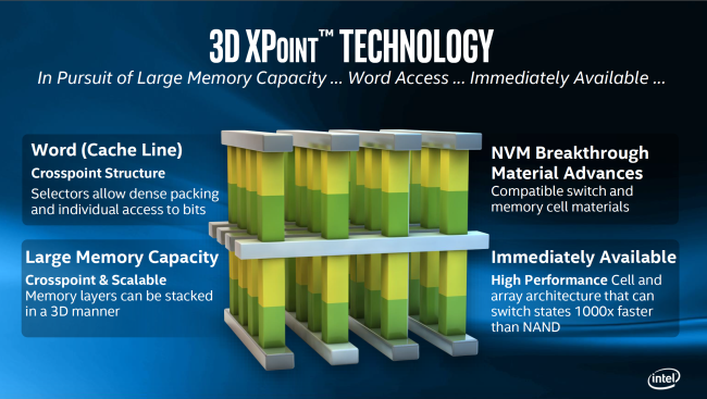
Also in the second half of last decade, Intel and Micron started talking about and then shipping Optane SSDs and DIMMs. Optane is based on what the companies call 3D XPoint, a form of phase-change memory (PCM). 3D XPoint also uses stacking (hence the name 3D), but the first generation is just two layers higher. The upcoming second generation 3D XPoint will double this to four layers.
Article continues belowOne major difference and advantage of 3D NAND, is that many layers can be processed simultaneously, so that the cycle time of producing a 3D NAND chip or wafer wouldn’t be, for example, 96 times longer than a single layer. However, this is exactly the case for 3D XPoint, where each layer has to be processed individually. Although that does not outright double the cost of the whole chip (or quadruple for four layers), it does mean that 3D XPoint’s scaling prospects to a large number of layers is limited.
3D NAND does have an analogue to 3D XPoint’s scaling challenges, called string stacking. In this technique, individually processed stacks of 3D NAND are stacked. For instance, Intel and Micron use it at 64 and 96 layers to stack two 32- or 48-layer stacks.
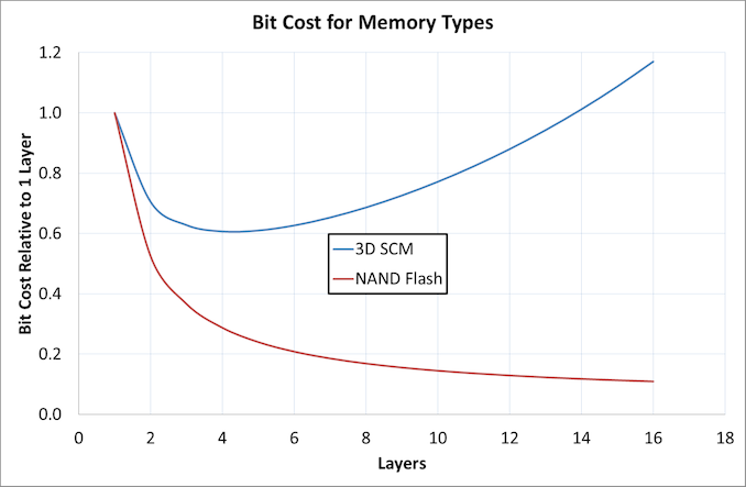
The above is the gist of Kioxia’s ‘assault’ on 3D XPoint and similar storage-class memories. At IEDM, the company showed following graph that has been reproduced by AnandTech (it was not allowed to take pictures).

The graph shows the bit cost of function of the number of layers of 3D SCM or NAND flash, normalized compared to one layer of the memory. As expected, for 3D NAND the advantages of scaling are impressive, yielding a ~10x cost per bit reduction for 16 layers.
Get Tom's Hardware's best news and in-depth reviews, straight to your inbox.
On the other hand, storage-class memory doesn’t fare very well, and even starts increasing beyond four layers, and hits cost-per-bit parity with a single layer at 14 layers. At its most efficient point of four layers, it yields a 40% bit cost reduction, much higher than 3D NAND’s ~70% cost reduction at 4 layers.
Several reasons for such increased cost include added complexity of scaling more layers, the inefficiency of having to process each layer individually, area lost due to more complex control circuitry and lower yield. For 64 layers, the cost per bit would be 50x higher per layer, at least according to the formula that Kioxia used.
As a note of caution, Kioxia likely does not have access to Intel or Micron's internal data, and its own SCM research also likely would not have progressed as far as those companies.
Intel and Micron have not given much information about their roadmaps, so it will have to be seen to how many layers the companies plan to scale 3X XPoint. The first generation started shipping in early 2017 after some delays, and the second generation with four layers will ship this year.
Besides scaling the number of layers, though, the companies have stated that 3D XPoint can also be scaled through conventional lithography, so that would present another scaling opportunity. Scaling 3D XPoint's feature sizes would even improve the its characteristics. A third scaling vector, in principle at least, would be to increase the number of bits per cell. In 3D NAND, companies are currently shipping up to quad-level cells (QLC), with 5-bit cells in research.
-
bit_user First, I don't see why SCM couldn't also be scaled in the same way as 3D NAND.Reply
Second:
A third scaling vector, in principle at least, would be to increase the number of bits per cell.
I'm not sure about that. NAND can scale the number of bits per cell, because it's analog (i.e. charge storage). Can SCM be treated as analog? If not, then you only get one bit per cell.
Also, packing more bits per cell would slow down SCM, if it were possible. So, I wouldn't even want it. For me, SCM's main selling point is its speed. -
jimmysmitty Company: "3DXpoint and other 3D NAND is not the way to go...."Reply
Also Company: "BTW here is our stuff...."
I get their argument but it really feels like they are just doing the normal "My idea is better" marketing. -
mradr Other than layering - flash NAND has already hit its limit for how many bits per cell we can deal with without it failing over night or getting any slow. Same with getting any smaller as the cell just keeps losing more and more life. If Xpoint can still scale from where it is now - even taking a bit of a hit in speed -it would still out last what flash NAND can do now.Reply
I don't follow why Xpoint can't do more than one layer though - that seems like a false statement? Sounds more like they just haven't explore the idea yet than a real limitation. Heck they could even do layering over layering for both tech and stacking on top of that by building layer one half way - work on layer 2 half way - then finally layer 3 half of layer 2 etc etc till a "stack" and then stack the stacks layer down the line.