Nvidia's Chinese A800 GPU's Performance Revealed
Nvidia's compute GPUs are so popular in China that they sell out quickly.

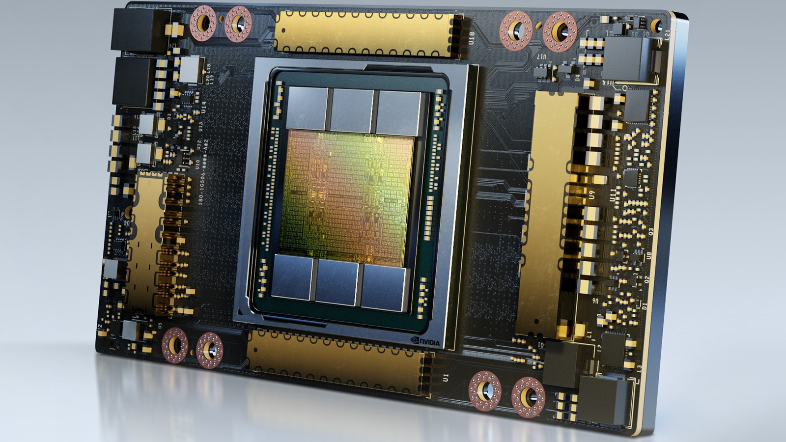
A rather brief story about overwhelming demand for Nvidia's high-performance computing hardware in China has revealed the performance of Nvidia's mysterious A800 compute GPU, which is made for the Chinese market. According to MyDrivers, the A800 operates at 70% of the speed of A100 GPUs while complying with strict U.S. export standards that limit how much processing power Nvidia can sell.
Being three years old now, Nvidia's A100 is quite a performer: it delivers 9.7 FP64/19.5 FP64 Tensor TFLOPS for HPC and up to 624 BF16/FP16 TFLOPS (with sparsity) for AI workloads. Even being cut by around 30%, these numbers will still look formidable: 6.8 FP64/13.7 FP64 Tensor TFLOPS as well as 437 BF16/FP16 (with sparsity).
Despite 'castration', (performance caps) as MyDrivers puts it it, Nvidia's A800 is quite a rival against fully-blown China-based Biren's BR104 and BR100 compute GPUs in terms of compute capabilities. Meanwhile, Nvidia's compute GPUs and its CUDA architecture are widely supported by applications run by its customers, whereas Biren's processors yet have to be adopted. And even Biren cannot ship its fully-fledged compute GPUs to China due to the latest regulations.
Article continues below| Row 0 - Cell 0 | Biren BR104 | Nvidia A800 | Nvidia A100 | Nvidia H100 |
| Form-Factor | FHFL Card | FHFL Card (?) | SXM4 | SXM5 |
| Transistor Count | ? | 54.2 billion | 54.2 billion | 80 billion |
| Node | N7 | N7 | N7 | 4N |
| Power | 300W | ? | 400W | 700W |
| FP32 TFLOPS | 128 | 13.7 (?) | 19.5 | 60 |
| TF32+ TFLOPS | 256 | ? | ? | ? |
| TF32 TFLOPS | ? | 109/218* (?) | 156/312* | 500/1000* |
| FP16 TFLOPS | ? | 56 (?) | 78 | 120 |
| FP16 TFLOPS Tensor | ? | 218/437* | 312/624* | 1000/2000* |
| BF16 TFLOPS | 512 | 27 | 39 | 120 |
| BF16 TFLOPS Tensor | ? | 218/437* | 312/624* | 1000/2000* |
| INT8 | 1024 | ? | ? | ? |
| INT8 TFLOPS Tensor | ? | 437/874* | 624/1248* | 2000/4000* |
* With sparsity
The export rules imposed by the United States in October 2021 prohibit the export of American technologies that allow for supercomputers with performance exceeding 100 FP64 PetaFLOPS or 200 FP32 PetaFLOPS within a space of 41,600 cubic feet (1,178 cubic meters) or less to China. While the export curbs do not specifically limit performance of each compute GPU sold to a China-based entity, they put curbs on their throughput and scalability.
After the new rules went into effect, Nvidia lost the ability to sell its ultra-high-end A100 and H100 compute GPUs to China-based customers without an export license, which is hard to get. In a bid to satisfy demand for the performance required by Chinese hyperscalers, the company introduced a cut down version of its A100 GPU dubbed the A800. Up until now, it was not clear how capable this GPU is.
As usage of artificial intelligence is increasing both among consumers and businesses, the popularity of high-performance hardware that can handle appropriate workloads is booming. Nvidia is among the main beneficiaries of the AI megatrend, which is why its GPUs are in such high demand that even the cut-down A800 is sold out in China.
Get Tom's Hardware's best news and in-depth reviews, straight to your inbox.
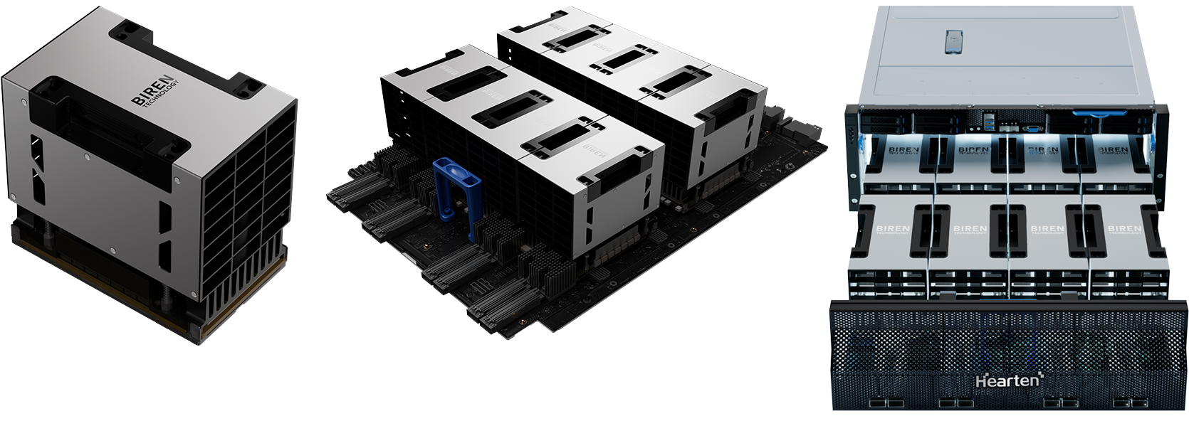
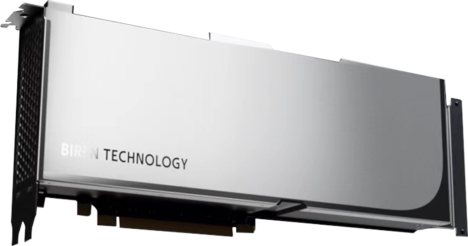
Biren's BR100 will be available in an OAM form-factor and consume up to 550W of power. The chip supports the company's proprietary 8-way BLink technology that allows the installation of up to eight BR100 GPUs per system. In contrast, the 300W BR104 will ship in a FHFL dual-wide PCIe card form-factor and support up to 3-way multi-GPU configuration. Both chips use a PCIe 5.0 x16 interface with the CXL protocol for accelerators on top, reports EETrend (via VideoCardz).
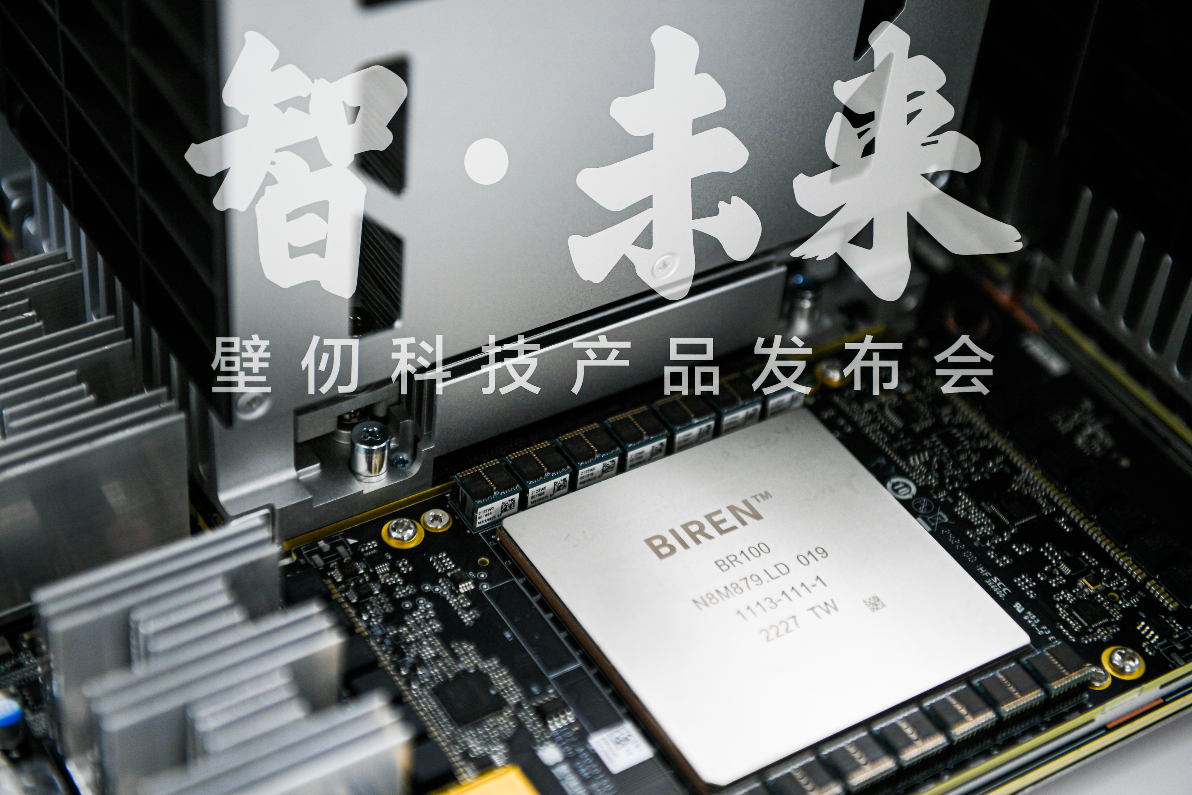
Biren says that both of its chips are made using TSMC's 7nm-class fabrication process (without elaborating whether it uses N7, N7+, or N7P). The larger BR100 packs 77 billion transistors, outweighing the 54.2 billion with the Nvidia A100 that's also made using one of TSMC's N7 nodes. The company also says that to overcome limitations imposed by TSMC's reticle size, it had to use chiplet design and the foundry's CoWoS 2.5D technology, which is completely logical as Nvidia's A100 was approaching the size of a reticle and the BR100 is supposed to be even larger given its higher transistor count.
Given the specs, we can speculate that BR100 basically uses two BR104s, though the developer has not formally confirmed that.
To commercialize its BR100 OAM accelerator, Biren worked with Inspur on an 8-way AI server that will be sampling starting Q4 2022. Baidu and China Mobile will be among the first customers to use Biren's compute GPUs.

Anton Shilov is a contributing writer at Tom’s Hardware. Over the past couple of decades, he has covered everything from CPUs and GPUs to supercomputers and from modern process technologies and latest fab tools to high-tech industry trends.
-
lorfa Is the BR104 really doing 128 FP32 TFlops in a 300 W TDP? If so that's kind of impressive.Reply


