Samsung 3nm Chip Mass Production On Track To Start in Q2
Samsung to kick off 3GAE mass production in Q2 2022.

Samsung on Thursday said that it is on track to start high-volume production using its 3GAE (3 nm-class gate all-around early) fabrication process this quarter (i.e., in the coming weeks). The announcement not only marks the industry's first 3nm-class manufacturing technology, but also the first node to use gate-all-around field effect transistors (GAAFETs).
"Enhance technology leadership via world’s first mass production of GAA 3-nano process," a statement [PDF] by Samsung reads.
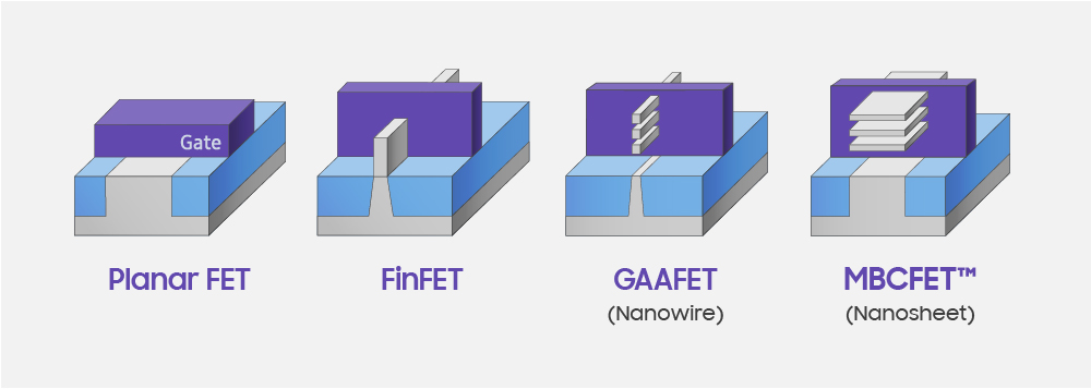
Samsung Foundry's 3GAE process technology is the company's first process to use GAA transistors, which Samsung officially calls multi-bridge channel field-effect transistors (MBCFETs).
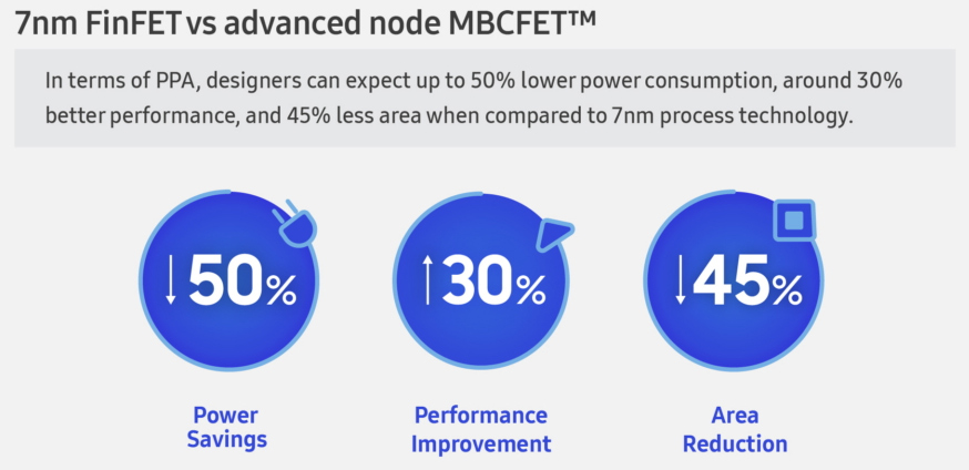
Samsung formally introduced its 3GAE and 3GAP nodes about three years ago. When the company described its 256Mb GAAFET SRAM chip produced using its 3GAE technology, it made a number of claims. Samsung said that the process would enable a 30% performance increase, a 50% power consumption reduction, and up to 80% higher transistor density (including a mix of logic and SRAM transistors). It remains to be seen how the actual combination of performance and power consumption will play out for Samsung though.
In theory, GAAFETs have a number of advantages when compared to currently used FinFETs. In GAA transistors, channels are horizontal and are surrounded by gates. The GAA channels are formed using epitaxy and selective materials removal, which allows designers to precisely tune them by adjusting width of the transistor channel. High performance is gained via wider channels, low power via narrower channels. Such precision greatly reduces transistor leakage current (i.e., lowers power consumption) as well as transistor performance variability (assuming that everything works well), which means faster time-to-yield, time-to-market, and improved yields. Also, GAAFETs promise to reduce cell area by 20% – 30%, according to a recent presentation by Applied Materials.
Speaking of Applied, it recently described high-vacuum IMS (Integrated Materials Solution) systems meant to address a major challenge of GAA transistor manufacturing: the necessity to deposit the multi-layer gate oxide and metal gate stacks around the channels in the tiny space available. The first new IMS tool from Applied Materials can deposit gate oxide that is 1.5 angstroms thinner using integrated atomic layer deposition (ALD), thermal, plasma treatment and metrology steps. The metal gate IMS integrates dipole engineering and a variety of ALD steps.
Samsung's 3GAE, being an 'early' 3nm-class manufacturing technology, 3GAE will be used primarily by Samsung LSI (Samsung's chip development arm) and perhaps one or two of SF's other alpha customers. Keeping in mind that Samsung's LSI and other early clients of SF tend to build chips in very high volumes, expect 3GAE technology to be used rather widely, assuming that yields and performance of those products meet expectations.
Get Tom's Hardware's best news and in-depth reviews, straight to your inbox.
Transiting to a brand-new transistor structure is generally a risk as it involves a brand-new fabrication process as well as all-new tools. Other challenges are new placement methodologies, floorplan rules, and routing rules that are introduced by all new nodes and addressed by new electronic design automation (EDA) software. Finally, chip designers need to develop all-new IP, which is expensive.

Anton Shilov is a contributing writer at Tom’s Hardware. Over the past couple of decades, he has covered everything from CPUs and GPUs to supercomputers and from modern process technologies and latest fab tools to high-tech industry trends.
-
-Fran- It would be interesting to check how TSMC positions its 5, 4 and 2nm nodes against 7nm to compare against Samsung's claims. I can't remember from the top of my head, but they were about 20% improvements per jump or so? So 7nm to 2nm (when it's ready) should be about ~50% better overall?Reply
Regards. -
watzupken The question is how is the yield? Mass production with 20% yield is not quite “mass” production.Reply -
InvalidError Reply
It can be if the things being manufactured have sufficient value to be economically viable at that level. Not an issue for things like medical, research, military, aerospace, telecom and industrial markets with nearly infinite budget for bleeding-edge stuff. Although it may not be billions of chips per year, the volumes can still be significant.watzupken said:The question is how is the yield? Mass production with 20% yield is not quite “mass” production. -
isofilm ReplyInvalidError said:It can be if the things being manufactured have sufficient value to be economically viable at that level. Not an issue for things like medical, research, military, aerospace, telecom and industrial markets with nearly infinite budget for bleeding-edge stuff. Although it may not be billions of chips per year, the volumes can still be significant.
Samsung has admitted to lying about their process yields, which for the 4nm are 30% after more than a year of tweaking, even though they falsely claimed 70%.
Now you expect us to believe Samsung has miraculously resolved their 3nm yields with its never before fabricated GAA design problems, with a current yield of ~10%?
Wafer yields under 45% are a loss, given traditional foundry margins of 45%. -
isofilm More information about Samsung’s pathetic failure.Reply
https://koreajoongangdaily.joins.com/2022/04/27/business/tech/Samsung-Electronics-foundry-3-nanomter-chip/20220427183621974.html


