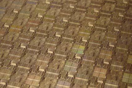
Researchers Create 22nm Indium Gallium Arsenide Transistors
Indium gallium arsenide is gaining traction as a potential successor of silicon in semiconductors.
Get Tom's Hardware's best news and in-depth reviews, straight to your inbox.
You are now subscribed
Your newsletter sign-up was successful
Following a 20 nm transistor announcement from Purdue University, researchers at MIT's Microsystems Technology Laboratories said they successfully created a 22 nm indium gallium arsenide compound transistor.
As semiconductor manufacturing processes transition to smaller structures, researchers believe that Silicon will eventually hit a limit at which it cannot be scaled anymore. Indium gallium arsenide is considered a potential candidate to replace silicon at the 10 nm and below level. MIT said that the material is already used in fiber-optic communication and radar technologies, and is known to have extremely good electrical properties. Recent successes to shrink transistors using the compound suggest that the industry is working toward a viable solution. The 10 nm mark is expected to be reached and surpassed in semiconductor manufacturing in the 2017/2018 time frame.
"We have shown that you can make extremely small indium gallium arsenide MOSFETs with excellent logic characteristics, which promises to take Moore's Law beyond the reach of silicon," said Jesús del Alamo, co-developer of the transistors.
Article continues belowThe researchers said that many of the techniques used to make the indium gallium arsenide transistors are in use in current silicon-based chip manufacturing. Even if the techniques have not been used for compounds, del Alamo believes that current production technologies need to be adopted.
"When you are talking about integrating billions of tiny transistors onto a chip, then we need to completely reformulate the fabrication technology of compound semiconductor transistors to look much more like that of silicon transistors," del Alamo said.
He said that the team will now be focusing on improving the electrical performance of their transistors, and further shrink the transistor gate length down to 10 nm.
Contact Us for News Tips, Corrections and Feedback
Get Tom's Hardware's best news and in-depth reviews, straight to your inbox.

Wolfgang Gruener is an experienced professional in digital strategy and content, specializing in web strategy, content architecture, user experience, and applying AI in content operations within the insurtech industry. His previous roles include Director, Digital Strategy and Content Experience at American Eagle, Managing Editor at TG Daily, and contributing to publications like Tom's Guide and Tom's Hardware.
-
deksman Sythentic diamonds and carbon nanotubes could have been used in late 1990-ies to go lower than what they are indicating (10nm).Reply
Besides, Graphene was stated to be ideal to go lower than 10nm.
The only reason we are seeing talks of this kind of reduction NOW is because its cheaper than it was over a decade ago from a $$ point of view, even though we had the technology and resources to do it back then - it just wasn't 'cost friendly').
Money is slowing all of this down on the commercial end - its disgusting.
-
clonazepam Replythe team will now be focusing on improving the electrical performance of their transistors...
Does that mean its electrical performance isn't on par with silicon yet? Or, unspecified? -
A Bad Day clonazepamDoes that mean its electrical performance isn't on par with silicon yet? Or, unspecified?Reply
What's wrong with making the electrical performance better than silicon? -
IndignantSkeptic @deksman, what social system do you suggest for getting technology to advance at a faster rate? You say Capitalism is the problem, but why?Reply
Anyway, question for anyone, can this chip material be recycled from older chips to make newer chips? -
pjmelect As I understand it Indium Gallium Arsenide can be used to make much faster devices than silicon. I have always wondered why it was not used instead of silicon in making processors. The reason I have been told is that Indium Gallium Arsenide is much more expensive to make.Reply -
A Bad Day deksmanSythentic diamonds and carbon nanotubes could have been used in late 1990-ies to go lower than what they are indicating (10nm).Besides, Graphene was stated to be ideal to go lower than 10nm.The only reason we are seeing talks of this kind of reduction NOW is because its cheaper than it was over a decade ago from a $$ point of view, even though we had the technology and resources to do it back then - it just wasn't 'cost friendly').Money is slowing all of this down on the commercial end - its disgusting.Reply
If you can't convince investors that you can make a marketable product, then tough luck.
There are some technologies that need decades of research before it's marketable, such as Li-ion batteries or LCDs.
