Regaining America's Supercomputing Supremacy With The Summit Supercomputer
Get Tom's Hardware's best news and in-depth reviews, straight to your inbox.
You are now subscribed
Your newsletter sign-up was successful
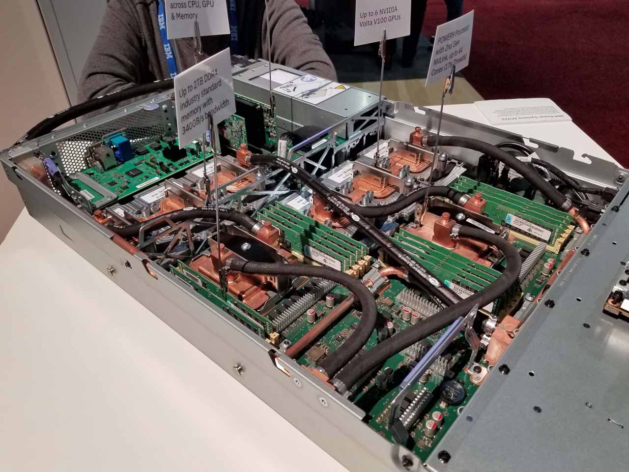
Oak Ridge National Laboratory's new Summit supercomputer, projected to be the fastest in the world, should rocket the U.S. back into the lead over China on the Top500 list of fastest supercomputers. At SuperComputing 2017, IBM demoed its Power Systems AC922 server nodes that serve as the backbone of the Summit supercomputer.
Summit will come online in 2018 with China's 93 PetaFLOPS Sunway TaihuLight, the world's fastest supercomputer, in its sights.
Summit will more than double Sunway's performance with ~200 PetaFLOPS. That's quite the achievement, considering the Sunway TaihuLight is ~60 PetaFLOPS ahead of the world's second-fastest supercomputer.
Article continues belowMuch like the rest of the industry, Supercomputing is evolving to AI-centric workloads. Summit's GPU-laden design is particularly well equipped for that role and should also provide up to 3 ExaFLOPS of performance for AI workloads.
Inside A Summit Node
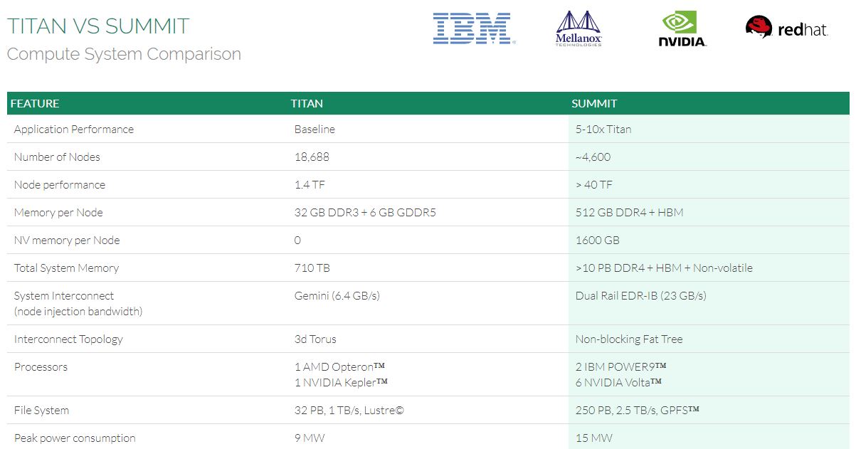
Summit promises to deliver 5-10x more performance than its predecessor, Titan, but it crams much more power into a smaller footprint. Titan featured 18,688 nodes, but Summit will overpower it with "only" ~4,600 nodes. That capability stems from increased node performance; Summit will offer more than 40 TeraFLOPS per node, whereas each Titan node weighed in at 1.4 TeraFLOPS.
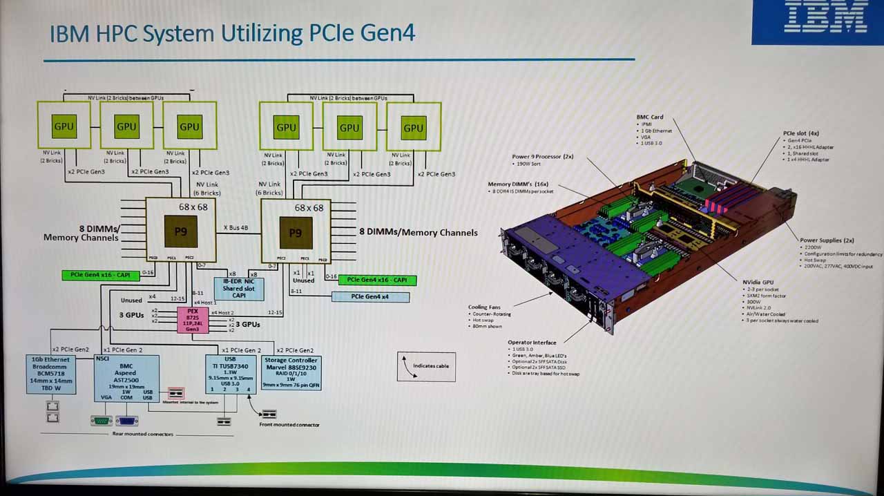
Packing all that power into a single node begins with IBM's water-cooled Power Systems AC922 node. Each node is equipped with two IBM POWER9 processors and six Nvidia Volta GV100 GPUs. The nodes also feature an aggregate of 512GB of coherent DDR4 and HBM2 (High Bandwidth Memory) along with 1,600GB of non-volatile RAM.
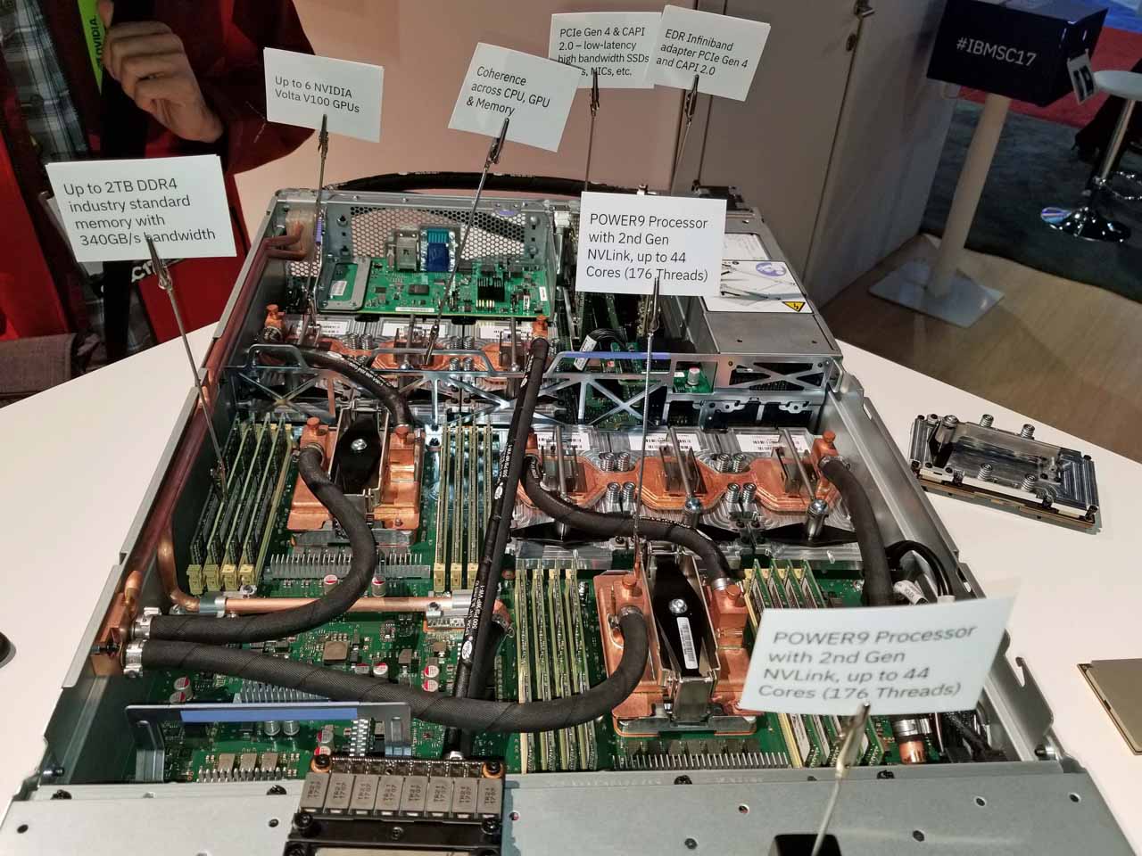

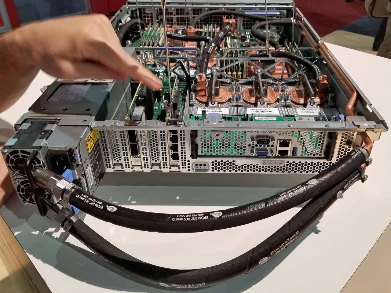

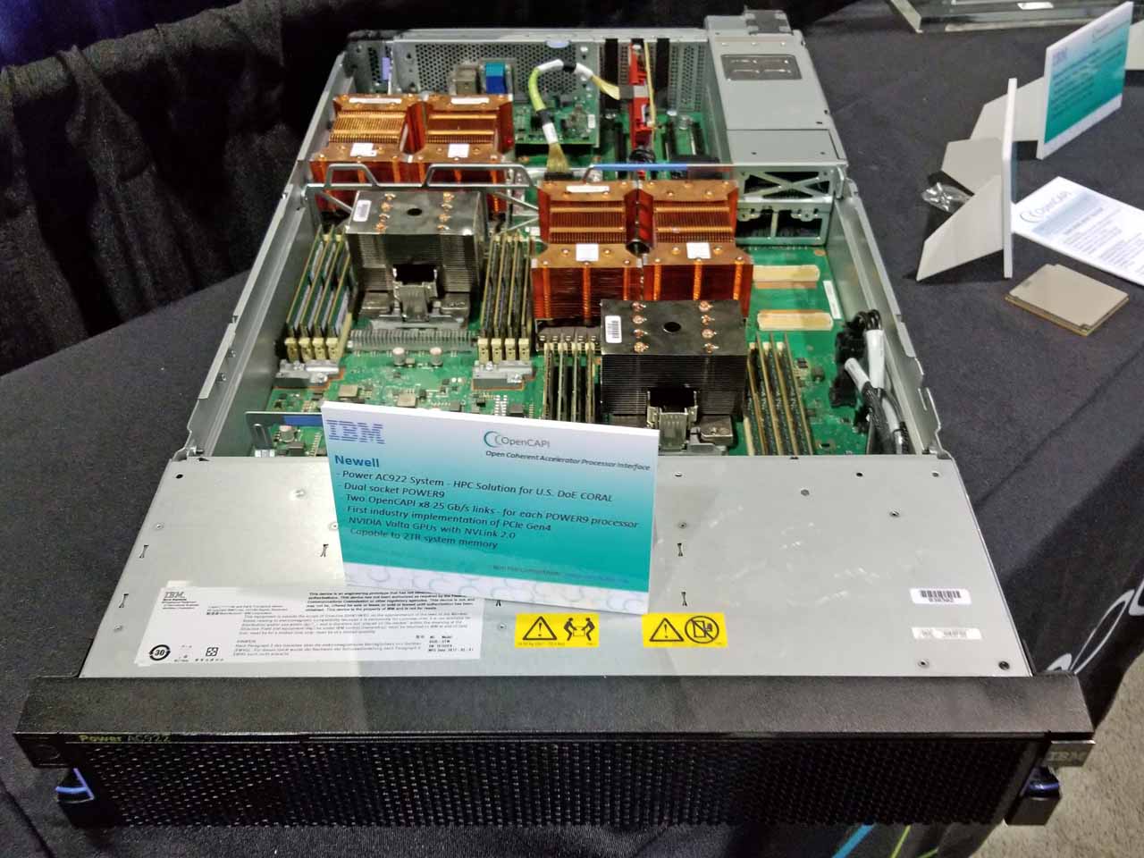
Supercomputers are all about parallel computation and moving data between the CPUs, GPUs, memory, and networking, so Summit provides numerous layers of extreme bandwidth.
Get Tom's Hardware's best news and in-depth reviews, straight to your inbox.
The system features 96 lanes of PCIe 4.0 that comes in handy for the dual-port Mellanox EDR InfiniBand adapter, which has a theoretical maximum throughput of 400Gb/s. IBM has measured throughput at 392Gb/s, which is twice the bandwidth of a PCIe 3.0 adapter.
The Volta GV100's connect via PCIe 3.0 and NVLink 2.0. The NVLink interface provides 100GB/s of throughput for CPU-to-GPU and GPU-to-GPU traffic. The GPUs are arranged in a dual-mesh design.
Interestingly, IBM also produces a model with four GPUs that will power CORAL's Sierra supercomputer. The four-GPU model (the last picture in the album above) touts 150GBps for inter-GPU/CPU communication. Due to the reduced number of GPUs, IBM can provision more links ("bricks" in NVLink parlance) to the CPUs and GPUs, which increases throughput.
The POWER9 processors have eight memory channels, for a total of 16 channels per server that provide 340GB/s of aggregate bandwidth. Each Summit node will wield a maximum of 2TB of DDR4-2666 memory.
Summit's 250 PB storage pool, which uses IBM's GPFS (General Parallel File System), spreads 2.5TB/s of bandwidth over all 4,600 nodes. Each node features 1,600GB of non-volatile RAM that serves as a burst buffer. The buffer absorbs bursts of data before transferring it to the remote primary storage pool. That helps sidestep the limited throughput allocation for each node.
Nvidia Volta GV100
Each Summit node features six Nvidia GV100 GPUs. We covered the GPUs in our A Closer Look At Nvidia's Volta article, so head there for more detail. In a nutshell, the Volta GV100 features a massive 815mm2 Volta die that wields 21 billion transistors built on TSMC's 12nm FFN process. It's complemented by four stacks of HBM2 (16GB total). Nvidia ships the GPU with 80 activated SMs (5,120 CUDA cores).
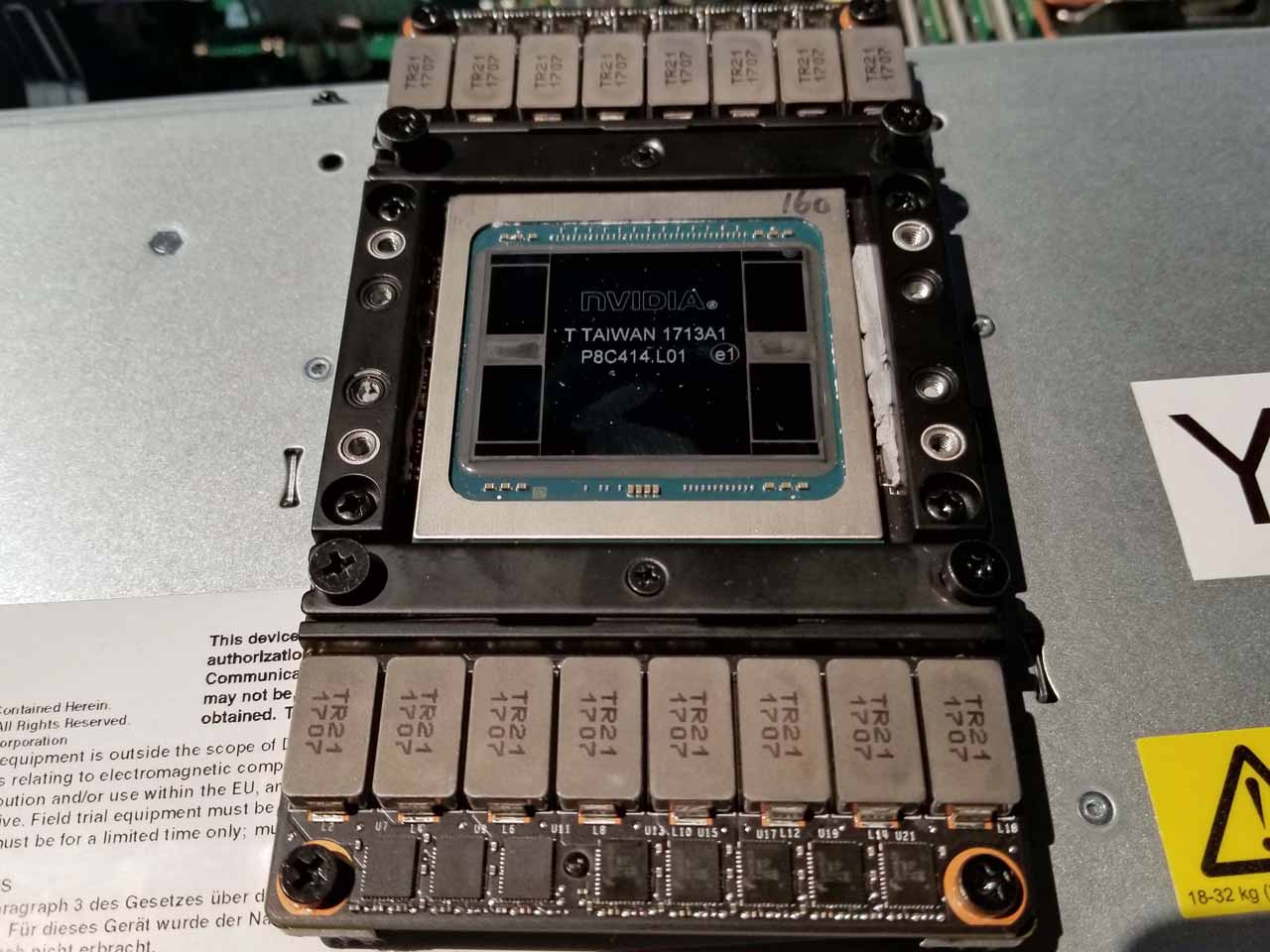
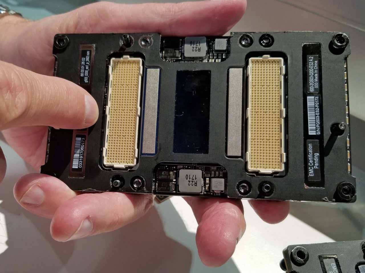
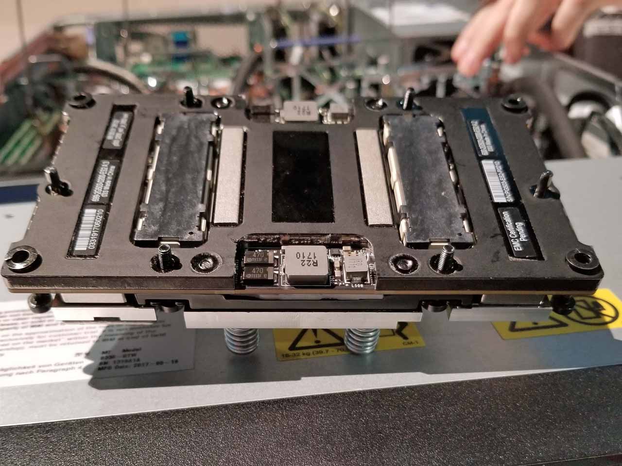
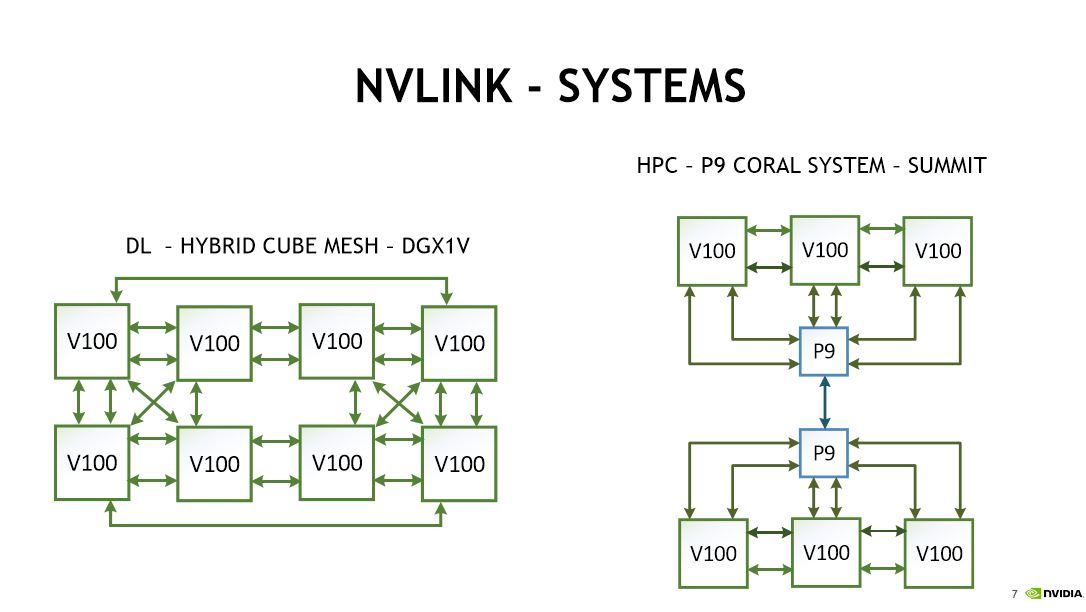
The Summit node features up to 2TB of coherent memory that can be accessed by either the GPU or CPU, so bandwidth is a critical requirement. Nvidia equipped the bottom of the GV100 with two mezzanine connectors. One connector provides power and accommodates PCIe and sideband traffic, while the other is dedicated to the NVLink 2.0 connection. NVLink is a separate interface that provides 6X the bandwidth of a PCIe 3.0 x16 connection. IBM's POWER9 processors have an integrated NVLink 2.0 connection on the processor.
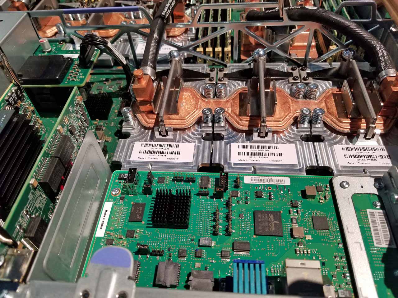
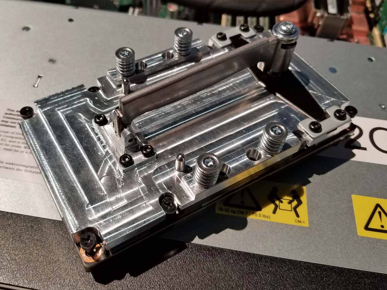
The Volta package pulls an average of 300W at a little below 1V, so over 300A flows into the die. That requires a beefy cooling solution. As with all the other primary compute components inside the node, the GV100s are watercooled. We can see the hefty waterblock and the holes (next to the spring-equipped fasteners) where the bridge, which spans groups of three GV100's, connects into the block.
The IBM POWER9 Processor
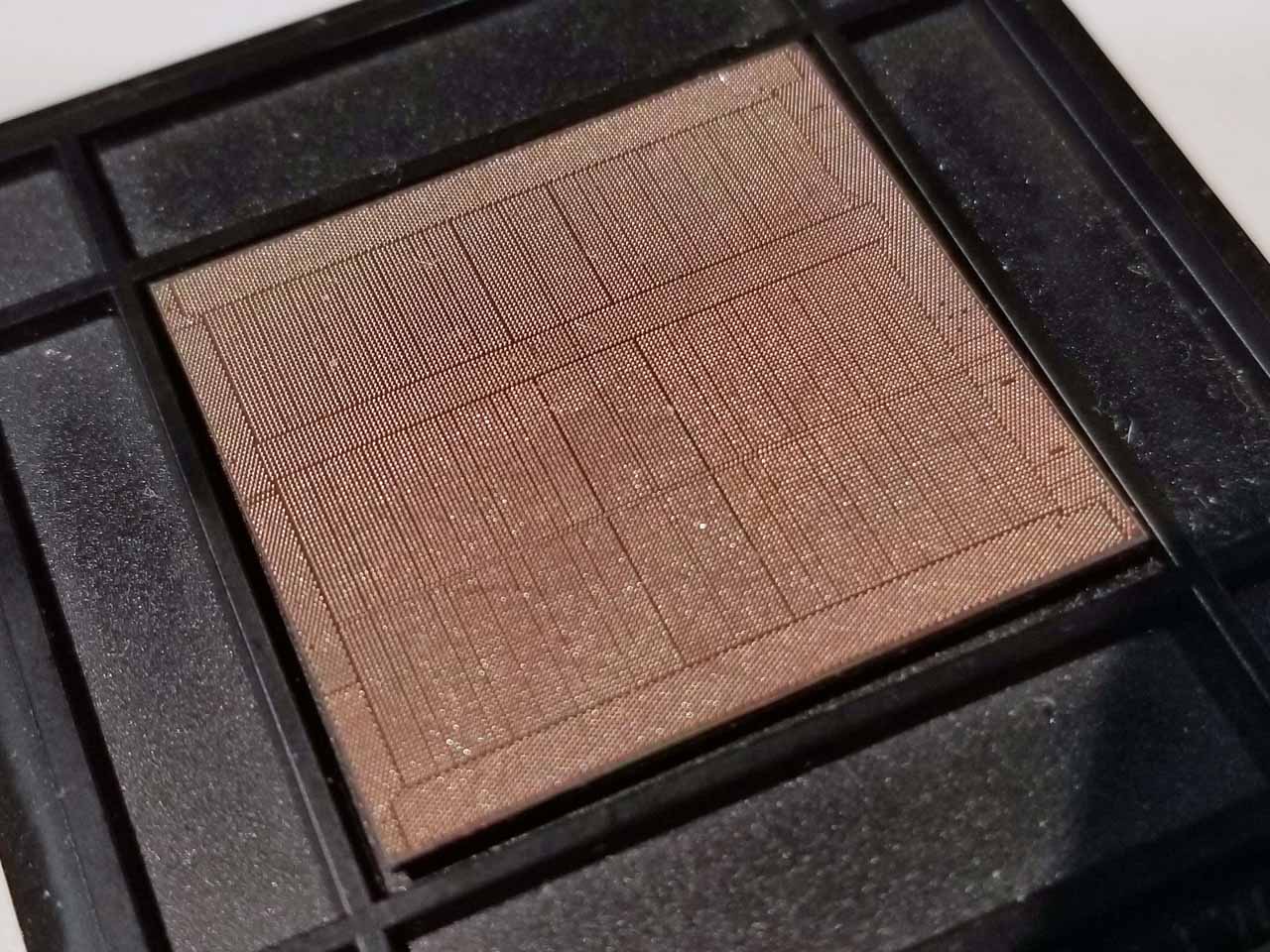
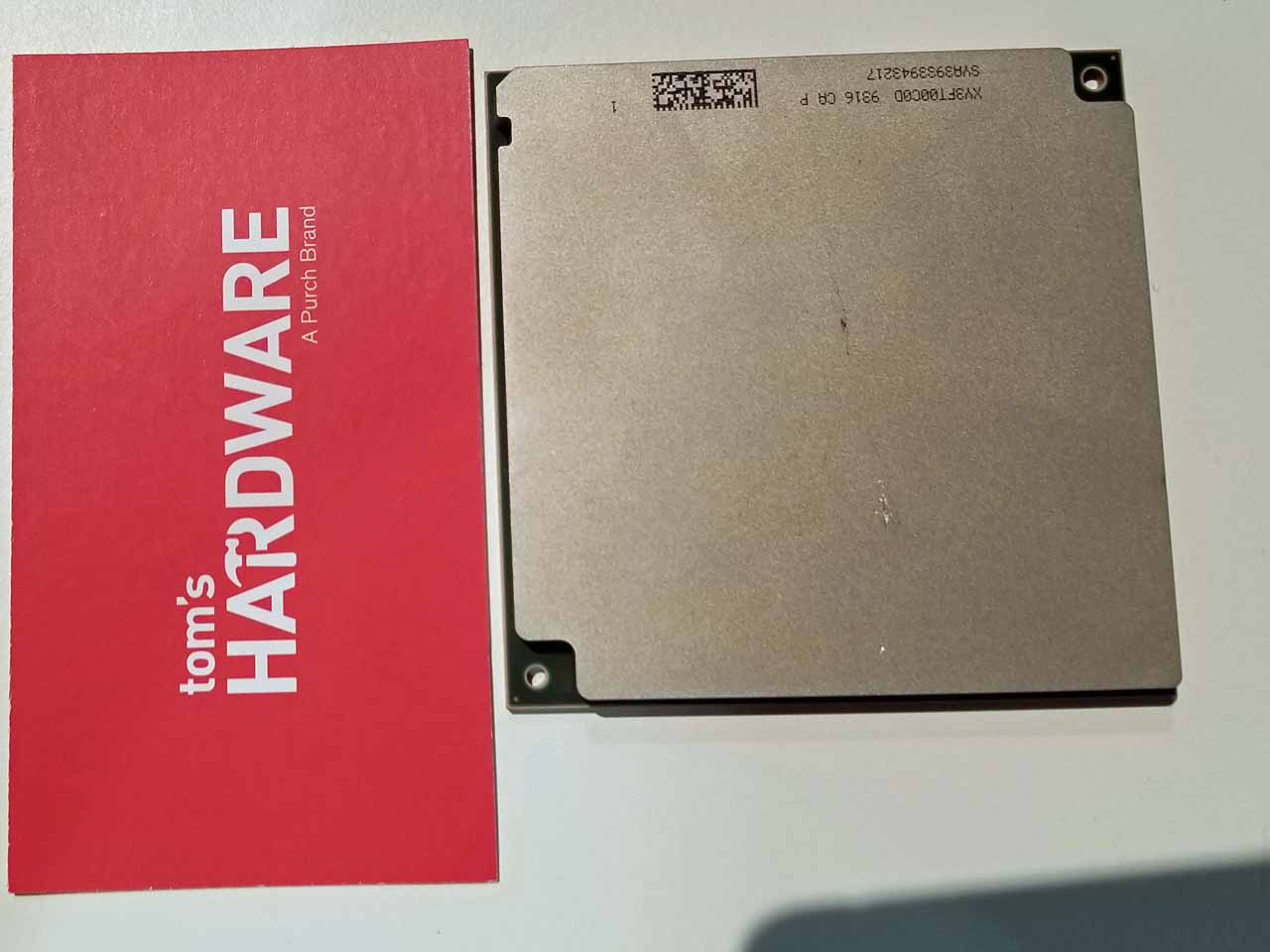
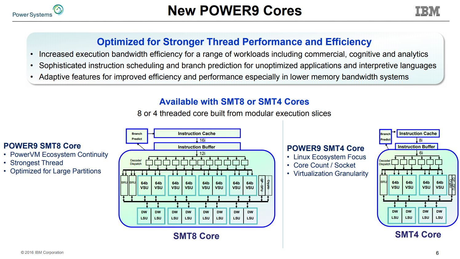
AI workloads shift the majority of the compute to the GPU, but the CPU still serves as the quarterback for data processing and movement. IBM's POWER9 is uniquely well-equipped for the role. IBM's POWER9-SO (Scale-Out) processor is built on Global Foundries' 14nm FinFET process and boasts 8 billion transistors. That large die requires a massive CPU package, which we've highlighted with our standard-sized business card. The processor features up to 24 cores that execute 96 threads. Each core executes four threads in parallel (SMT4), while the 12-core model executes eight threads per core (SMT8).
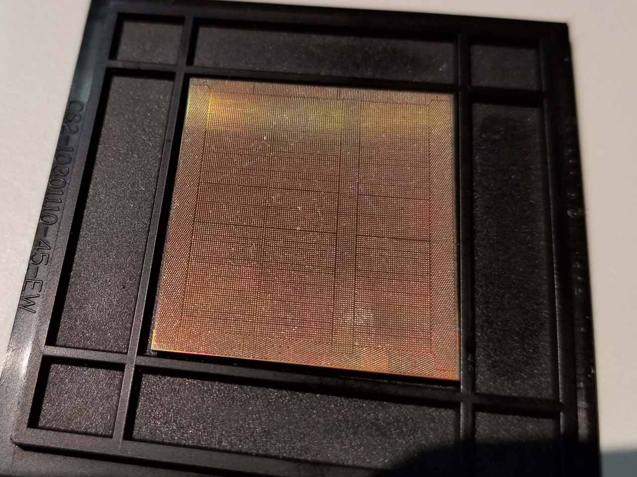
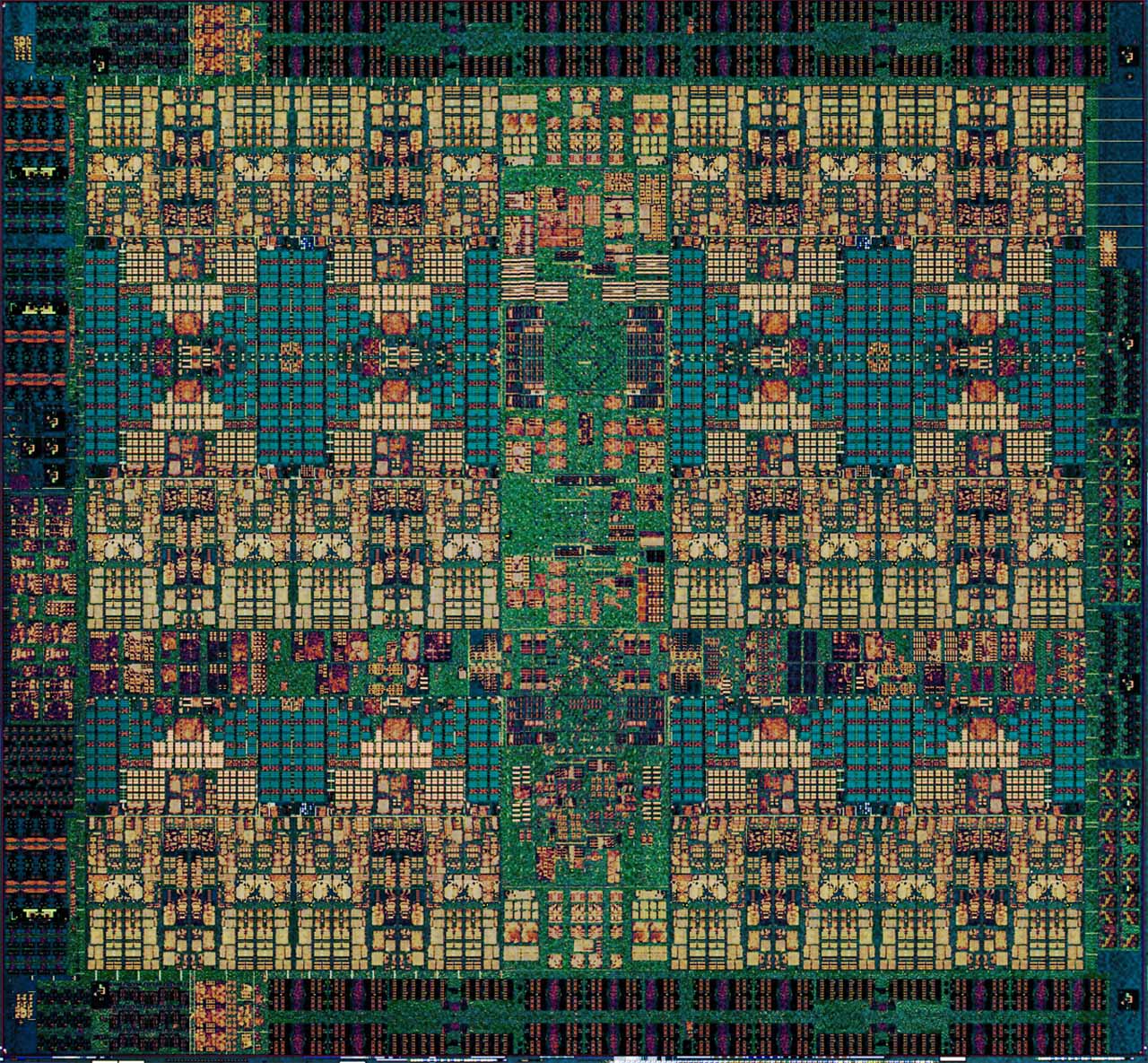
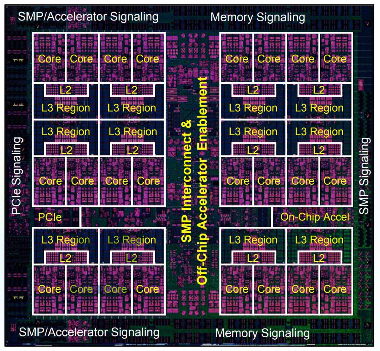
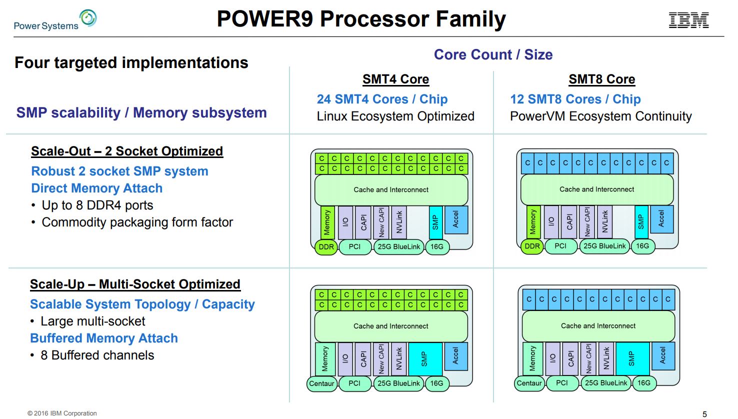
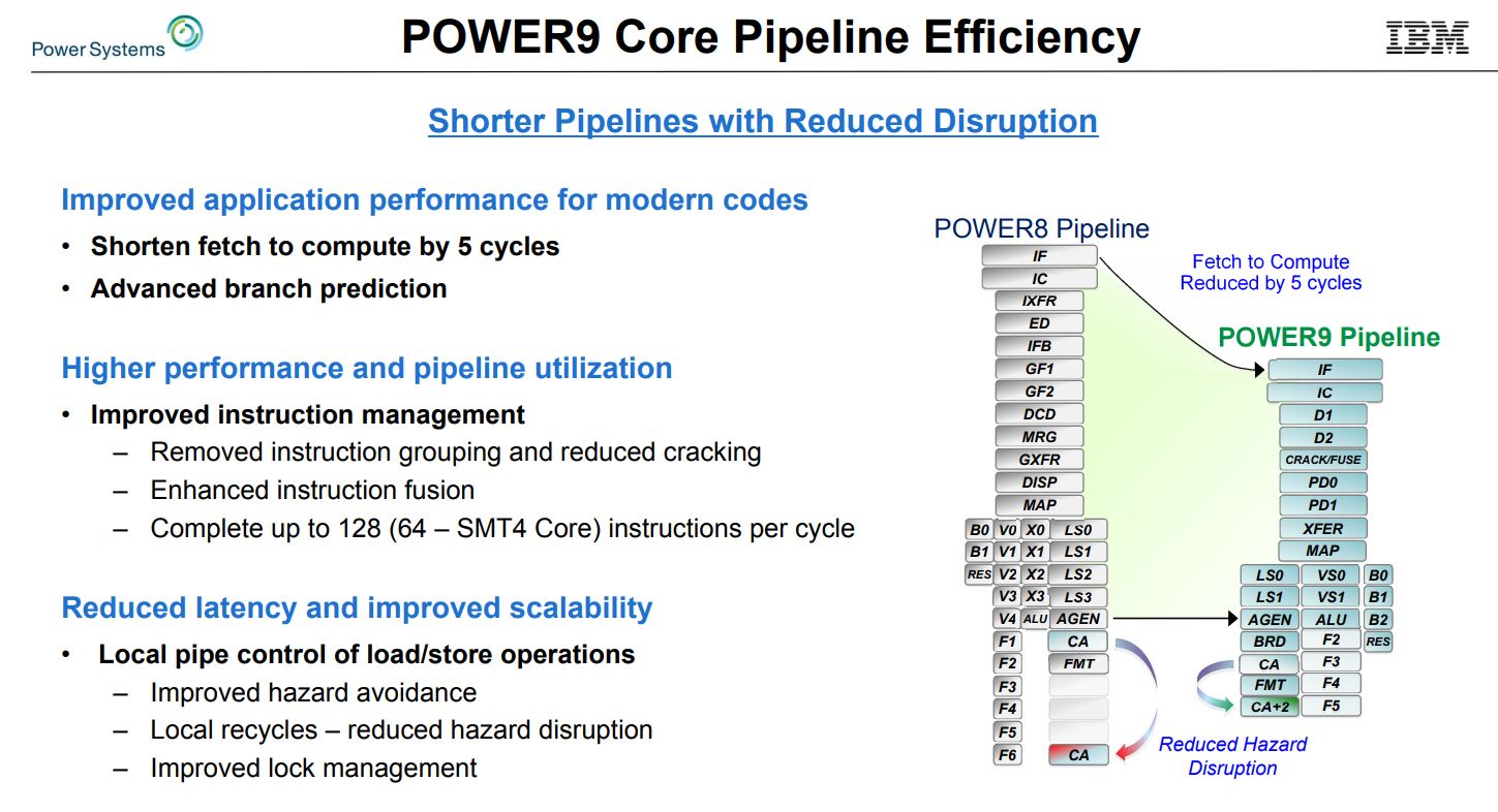
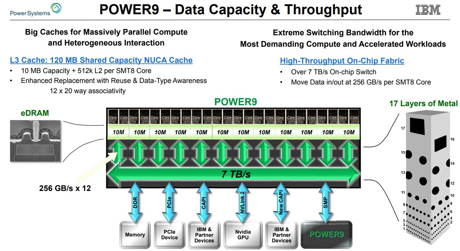
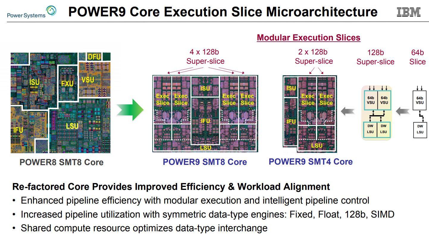
Each processor provides 48 lanes of PCIe 4.0 that deliver 192GB/s of duplex bandwidth, and eight memory channels support up to 4TB of DDR4-2666 memory per socket with 120GB/s of sustained bandwidth.
The processor also boasts 120MB of shared L3 eDRAM cache (10MB blocks shared between groups of two cores) with up to 256GB/s of throughput per core.
The processor also has support for Nvidia's NVLink 2.0 and CAPI 2.0 integrated into the die. Cache, memory, PCIe, and NVLink traffic (among others) all flow through the processor, which requires a strong fabric. IBM infused the processor with a 7TB/s on-chip fabric.
Reaching The Summit
The Summit supercomputer will consume 15MW of power, which is on-par with China's Sunway. That's a notable increase from Titan's 9MW, but considering the massive leap in performance, it's surprisingly efficient. Summit also has room to grow; the site has a 20MW overall power budget. The entire Summit supercomputer will consume a space roughly the size of two basketball courts and require 136 miles of cabling.
The system is on-schedule for deployment in 2018, and barring a dark horse entrant, it should propel the U.S. back into the supercomputing lead.

Paul Alcorn is the Editor-in-Chief for Tom's Hardware US. He also writes news and reviews on CPUs, storage, and enterprise hardware.
-
Colin_10 This is kind of like the space race of a previous generation. Not sure what the end goal is here though, there doesn't seem to be a "Moon" to reach here, just more and more power.Reply -
Joao Ribeiro Hmmm, this seems it could improve if AMD's EPYC were to be used as it would allow 4 GPU's per socket easily and still have spare PCIe lanes... Hmmm, would really like to see a comparison between the two solutions as honestly I am not aware of enough tech details about the IBM's Power 9, still, from what I have gathered about EPYC from AMD it should allow for a more compatible (less emulation/translation layers and increased x86 support) and consequently higher performing solution due to better optimized code from the get go, but still I need more data to reach a definite conclusion. I would still place my bet on EPYC at this stage against IBM's Power 9, which I must say I praise (in part due to it's heritage, but against practical results nothing competes)Reply -
bit_user Someone needs to write a game engine that efficiently utilizes even one whole chassis, let alone a rack or the entire thing. That could be impressive.Reply -
kyotokid Reply
..one downside of Epyc, it doesn't support full NVLink, only x86 so it would use the narrower PCIe pipeline. between the CPU and GPUs. Only the IBM Power 8 and 9 series CPUs are capable of full NVLink.20398263 said:Hmmm, this seems it could improve if AMD's EPYC were to be used as it would allow 4 GPU's per socket easily and still have spare PCIe lanes... Hmmm, would really like to see a comparison between the two solutions as honestly I am not aware of enough tech details about the IBM's Power 9, still, from what I have gathered about EPYC from AMD it should allow for a more compatible (less emulation/translation layers and increased x86 support) and consequently higher performing solution due to better optimized code from the get go, but still I need more data to reach a definite conclusion. I would still place my bet on EPYC at this stage against IBM's Power 9, which I must say I praise (in part due to it's heritage, but against practical results nothing competes)
