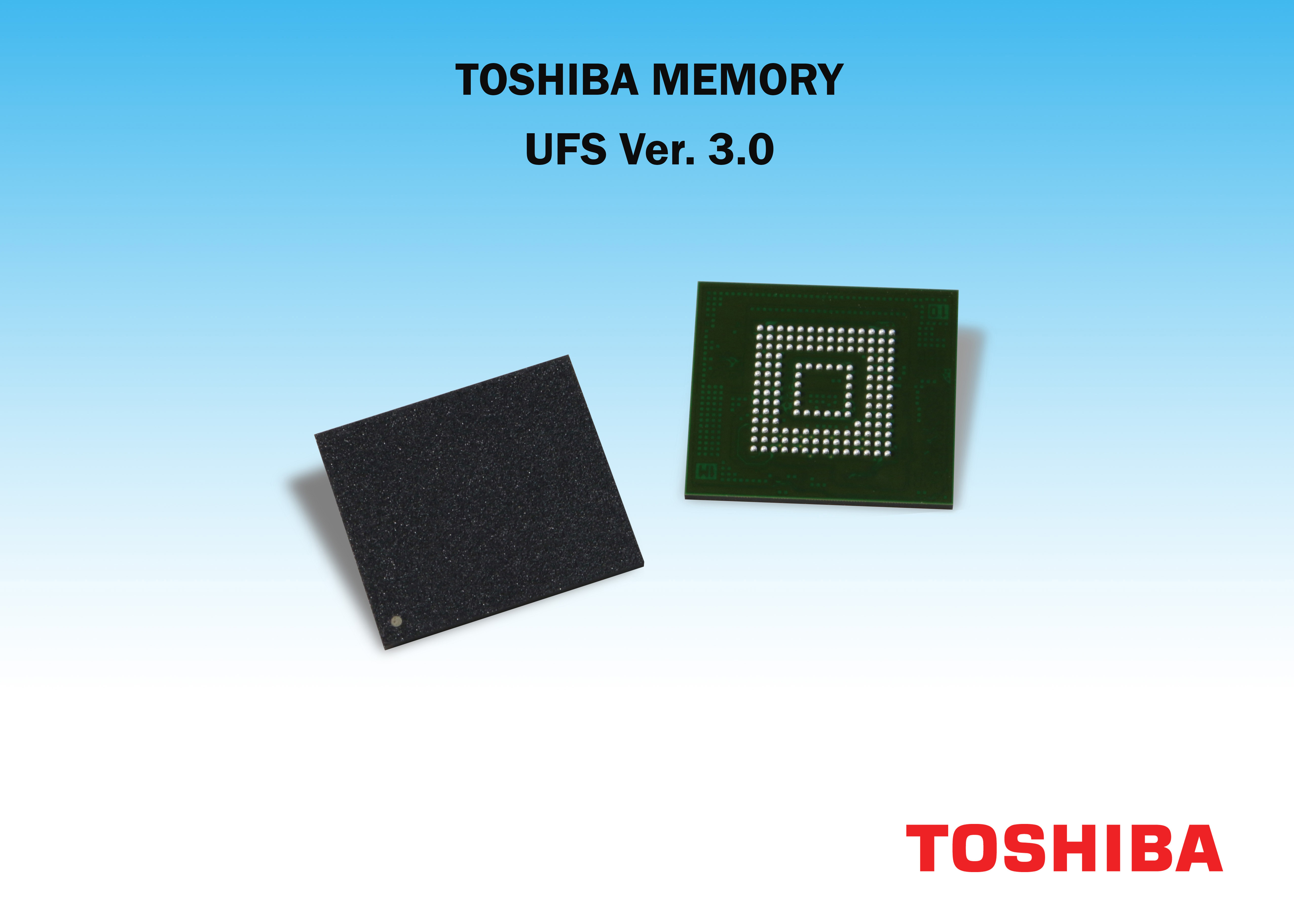
Toshiba Starts Sampling World’s First UFS 3.0 Embedded Flash Chips
Toshiba announced the industry’s first embedded flash chips to use the ultra-fast Universal Flash Storage (UFS) version 3.0 technology. The new memory chips target smartphones, tablets, and augmented/virtual reality systems.
Toshiba's UFS 3.0 Embedded Flash
Toshiba said that the new chips use the cutting-edge 96-layer BiCS FLASH, the company’s 3D flash memory technology, and a controller in a JEDEC-standard 11.5 x 13mm package. Chips will be made available in three capacities: 128GB, 256GB, and 512GB.
The controller performs error correction, wear leveling, logical-to-physical address translation, and bad-block management for simplified system development.
All three devices are compliant with JEDEC UFS 3.0, as well as the HS-GEAR4 standard, which has a theoretical interface speed of up to 11.6 Gigabits per second per lane. With two lanes, the chips can reach a peak interface bandwidth of 23.2Gbps (2.9GB/s).
Toshiba didn't disclose the read and write speed of the chips, but it noted that the 512GB drives will support an increased read and write performance over the previous generation of 70 percent and 80 percent, respectively.
Toshiba Bets on UFS
Toshiba is no stranger to JEDEC’s UFS memory standard, as it was also the first company to release UFS samples back in 2013, just as now, six years later, it’s the first to sample UFS 3.0 embedded memory chips.
The UFS standard has started to gain rapid adoption in smartphones over the past few years, as a higher-performance alternative to eMMC. Samsung and other companies have even started to use the standard for external memory cards, as an alternative to SD cards.
Get Tom's Hardware's best news and in-depth reviews, straight to your inbox.
Sampling of Toshiba’s 128GB chip started today, and smartphones using it are expected to ship later this year.
Lucian Armasu is a Contributing Writer for Tom's Hardware US. He covers software news and the issues surrounding privacy and security.
