
The U.S. Department of Commerce (DoC) has revealed the strategy on how it will spend the $50 Billion from the CHIPS for America Fund. The U.S. government will share the funds between makers of logic and memory who use leading-edge fabrication technologies, manufacturers of chips on mature or specialty process technologies that are used by the military or critical industries, as well as advanced R&D facilities. Each of the CHIPS money beneficiaries will have to meet numerous requirements.
The CHIPS for America program has several strategic goals: to attract leading-edge semiconductor manufacturing to the U.S., build-up a top-to-bottom chip supply chain to support chip production, establish a constellation of R&D programs that will design next-generation semiconductor products and technologies in private-public collaboration, and create good-paying manufacturing jobs. On the operational sides of things, the program is seeking to build strong public-private partnerships as well as attract private capital to the sector.
Leading Edge Manufacturing
Makers of chips who use the most advanced next-generation fabrication technologies will get the lion's share of the CHIPS for America Fund — $28 billion.
The funds will not be provided to interested parties only as grants (even though these will be key instruments in enabling companies to build new leading-edge fabs in the U.S.), but will also be available for cooperative agreements, or to subsidize loans or loan guarantees. The DoC stresses that to get subsidies from the government, manufacturers will have to substantiate that they need the subsidies money to make their investments, not substitute their own budgets with money from the taxpayers' pockets.
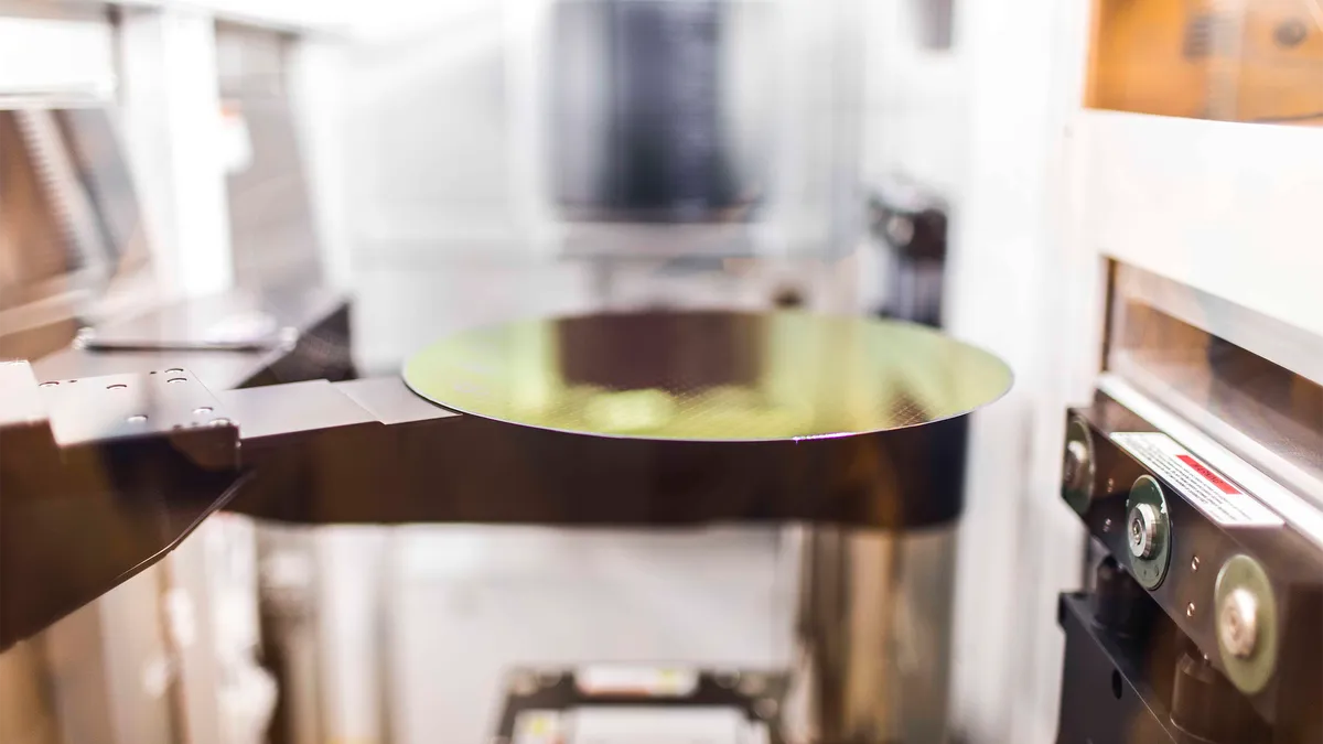
Under makers, the U.S. government considers not only companies that process wafers and fabricate silicon dies, but also OSAT (outsourced assembly and test) services providers. This is a particularly wise move as billion-dollar semiconductor facilities also require advanced OSAT plants and taking chips from the U.S. to Asia for test and packaging is not only expensive and time consuming, but is also risky given logistics and current geopolitical tensions. While classic/simple chip packaging services will mostly remain outside of the U.S. due to economic reasons, advanced packaging facilities (such as those that Intel intends to use with its EMIB and Foveros technologies) are encouraged to move to the U.S.
The DoC is seeking proposals for construction or expansion of the aforementioned manufacturing facilities and will give preferences to projects that involve multiple high-cost production lines and associated supplier ecosystems. Also, the DoC encourages companies seeking support from the Fund to get support from state and local authorities, get private investments or form collaborations with clients or suppliers. Actually, the department intends to prefer projects that receive state and local incentive packages to maximize economic effect.
In the recent quarters numerous companies, including Intel, Micron, Samsung Foundry, and TSMC announced plans to spend hundreds of billions of dollars to build new leading-edge fabs in the USA. In fact, Intel and Samsung have already begun building them and TSMC is on the finish line with its fab in Arizona. $28 billion will provide a great support to these companies, but the question is whether this will be enough?
Mature and Current Generation Manufacturing
The second category of companies to get support from the CHIPS for America Fund are foundries and chipmakers that use existing, mature, and specialty fabrication processes to make chips for defense and commercial sectors, such as automobiles, information and communications technology, and medical devices. This includes various advanced analog chips, radiation-hardened chips, compound semiconductors, and countless emerging ICs. Over time new packaging technologies will also be used for these applications.
Makers of those chips as well as their OSAT partners can collectively get $10 billion from the U.S. government under the same terms and conditions as makers of chips using leading-edge production nodes. The DoC expects these companies to expand or re-equip existing or build new fabs. In fact, GlobalFoundries invested $1 billion in expansion of its existing Fab 8 in New York in 2021, whereas Texas Instruments is building and equipping two fabs in Texas and one in Utah.
R&D Initiatives
Supporting research and development (R&D) in the U.S. is by all means as crucial as supporting local semiconductor manufacturing as without fundamental scientific breakthroughs there will be no new applied devices to produce. To properly manage R&D projects, the DoC split them into four major initiatives focusing on chip manufacturing, advanced semiconductor research, metrology research, and innovative chip packaging, which will together receive $11 billion in total.
One of the key enablers of advanced semiconductor R&D in the U.S. will be the National Semiconductor Technology Center (NSTC) that will deal with research and prototype of advanced semiconductor technologies. One of NSTC's key goals will be bringing together industry, government, national labs, and academia to conduct advanced semiconductor research and prototyping. Essentially, the U.S. government wants to establish an innovation network across the USA that will work on important semiconductor-related research projects aimed at the mid-term and long-term future. Furthermore, NSTC will be able to partner with partners from friendly foreign countries.
"The Department expects the NSTC to focus on advancing semiconductor design, scaling new manufacturing processes, developing new tools and materials, and improving the lab-to-fab product flow," a statement by the DoC reads.
The NSTC's role is to back development of standards and technical roadmaps to lead concurrent design of materials, production equipment, software, and actual products. While we expect companies to collaborate on pre-competitive R&D of materials, software, and tools, we do not expect them to work together on actual end-use applications. As demonstrated by joint development of 3D XPoint, not everyone can benefit from a new type of memory.
Another important direction organization that will be established will be the National Advanced Packaging Manufacturing Program (NAPMP). As the name implies, the program will focus on developing novel chip packaging methods and ensuring these methods are applied by fabs located in the U.S. Again, NAPMP will attempt to work together with scientists from academia and engineers from around the industry.
Both NSTC and NAPMP will be led by the director of the National Institute of Standards and Technology (NIST). Meanwhile, NIST will also be responsible for the nationwide Metrology Research program, which will focus on physical metrology required for next-generation semiconductors (including those that use various 3D transistors, such as gate-all-around FETs) as well as computational metrology that is used for application where traditional metrology methods are inapplicable. Also, it will work on virtualization and automation for for computationally intensive and data-driven aspects of semiconductor metrology. In addition, NIST's Metrology Research will also have to establish measurement and calibration services as well as measurement and documentary standards.
Finally, NIST will establish Manufacturing USA Institute, a network of semiconductor manufacturing, government, and academic organizations focused on chip R&D. The key idea is to provide members of those organizations access to state-of-the-art facilities and equipment to encourage R&D as well as train the workforce.
How Will It Work?
Given the scale of the CHIPS for America fund, there will be tens of companies seeking government subsidies (and other forms of support), so the DoC will have to build a mechanism to review applications and determine their benefits both in terms of technology and economics.

All requests will be reviewed by a team and the DoC is hiring around 50 people to review technical and financial merit of submissions, rationale for public funding, and operational capabilities of the applicant, according to NYTimes. The team is expected to begin seeking submissions within six months and is also expected to give feedback to potential recipients before they submit a complete applications.
The same team will monitor the use of funds and may recover funds if recipients fail to initiate or complete projects on time. Recipients will be prohibited to expand or build new semiconductor production capacity in China for 10 years after getting support from the CHIPS for America fund as well as use those money for stock buyback or dividend payments. The China issue may be a roadblock for Samsung's getting support from the CHIPS for America fund as the company has manufacturing capacity in Tianxia. Also, the DoC will track IP transactions of the fund's recipients as such deals may raise national security concerns.
Since the CHIPS for America program is designed to lure leading semiconductor manufacturers to the U.S. and reinvigorate resilient chip supply chain in the country, the DoC will prefer funding established players as well as R&D projects backed by reputable academia and private companies. Meanwhile, NSTC will attract research partners from around the world to advance the U.S. semi-industry.
Now that the strategy behind the CHIPS for America program is here and it is more or less understandable which companies are set to benefit from it, a new question that arises is how much those companies will get. We will learn this in the coming months.
