Intel Details 3D Chip Packaging Tech for Meteor Lake, Arrow Lake and Lunar Lake
Scaling silicon into the third dimension.
Intel revealed more new details about the 3D Foveros chip design it will use for its Meteor Lake, Arrow Lake, and Lunar Lake chips today as a teaser to the company's presentation at Hot Chips 34, a semiconductor industry conference that sees the titans of tech sharing the architectural details of their new processors. Intel CEO Pat Gelsinger will keynote the event, and the company also has four technical presentations, including the consumer 'Lake' processors we'll discuss here and Ponte Vecchio GPUs, FPGAs, and the Xeon D processors.
First and foremost, there have been recent rumors that Intel's Meteor Lake will be late to market due to Intel switching from the TSMC 3nm node to the 5nm node for its GPU tile/chiplet. While Intel still isn't sharing information about which specific node it will use for the GPU, company representatives say the planned node for the GPU tile has not changed, and the processor is on track for an on-time release in 2023. Notably, Intel will only manufacture one of the four tiles used to construct its Meteor Lake chips — TSMC will produce the other three. Industry sources indicate the GPU tile is TSMC N5 (5nm).
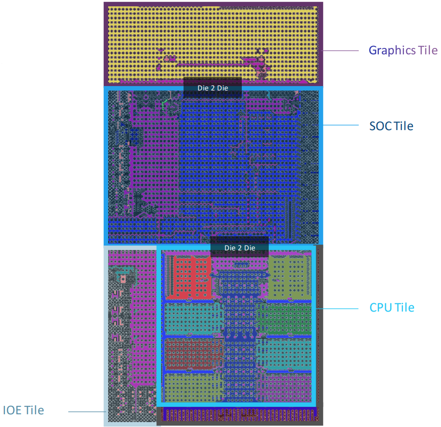
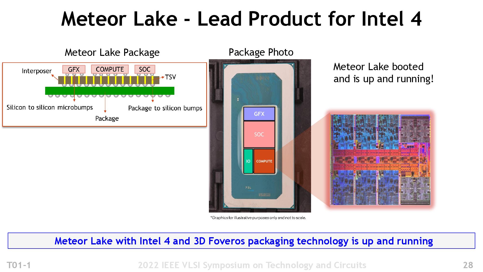
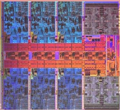
The first image in the above album is a new diagram that Intel shared of its Meteor Lake processors. We also added the following slides from our Intel 4 process node coverage. The new image has a few new details — Intel says this diagram is of a mobile processor that will ship to the market with six performance cores and two clusters of efficiency cores. Intel hasn't confirmed, but these are thought to feature the Redwood Cove and Crestmont architectures, respectively. Meteor Lake and Arrow Lake chips will scale to meet the needs of the mobile and desktop PC market, whereas Lunar Lake will serve the mobile 15W and under market.
Packaging and interconnect advancements are rapidly changing the face of modern processors. Both are now just as important as the underlying process node technology — and arguably more important in some facets.
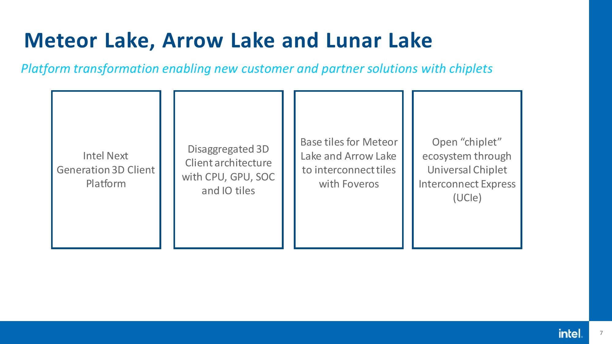
Many of Intel's disclosures today center around its 3D Foveros packaging tech that it will use as a bedrock for its Meteor Lake, Arrow Lake, and Lunar Lake processors for the consumer market. This technology allows Intel to stack chiplets vertically atop one unifying base die with a Foveros interconnect. Intel also uses Foveros for its Ponte Vecchio and Rialto Bridge GPUs and the Agilex FPGAs, so this is a foundational technology for several of the company's next-gen products.
Intel first brought 3D Foveros to market in its low-volume Lakefield processors, but the four-tile Meteor Lake and nearly 50-tile Ponte Vecchio are the company's first high-volume chip production with the technology. After Arrow Lake, Intel will transition to the new UCIe interconnect, thus tapping into the forming ecosystem of chiplets that use a standardized interface.
Intel revealed that it will place the four Meteor Lake chiplets (called 'tiles' in Intel parlance) on top of a passive Foveros interposer/base tile. The chiplets and interposer are wired together with TSV connections, and the interposer doesn't have any logic. The Meteor Lake base tile is different than the one found in Lakefield, which served as an SoC of sorts. The 3D Foveros packaging tech also supports active interposers. Intel says it manufactures the Foveros interposer with its low-cost and low-power-optimized 22FFL process (the same as Lakefield). Intel also has a newer 'Intel 16' variant of this node for its foundry services, but it isn't clear which version Intel will use for the Meteor Lake base tile.
Intel will mount the compute tile, which uses the Intel 4 process (more here), the I/O tile, the SoC tile, and the graphics tile (tGPU) atop this interposer. All of these units are Intel-designed and feature Intel architectures, but external foundry TSMC will manufacture the I/O, SoC, and GPU tiles. That means Intel will manufacture only the CPU and Foveros tiles.
Industry sources tell us that the I/O die and SoC are fabbed on TSMC N6, while the tGPU uses TSMC N5. (Notably, Intel calls the I/O tile an 'I/O Expander,' hence the IOE moniker.)
Get Tom's Hardware's best news and in-depth reviews, straight to your inbox.
| Intel Meteor Lake Tile/Chiplet | Manufacturer / Node |
| CPU Tile | Intel / 'Intel 4' |
| 3D Foveros Base Die | Intel / 22FFL (Intel 16) |
| GPU Tile (tGPU) | TSMC / N5 (5nm) |
| SoC Tile | TSMC / N6 (6nm) |
| IOE Tile | TSMC / N6 (6nm) |
Foveros uses a 36-micron bump pitch (a critical measurement of interconnect density), an improvement over the 55-micron bump pitch it used with Lakefield. The Foveros roadmap includes 25- and 18-micron pitches with future designs. In the future, Intel says it could theoretically even use hybrid bonding interconnects (HBI) to reach 1-micron bump pitches.
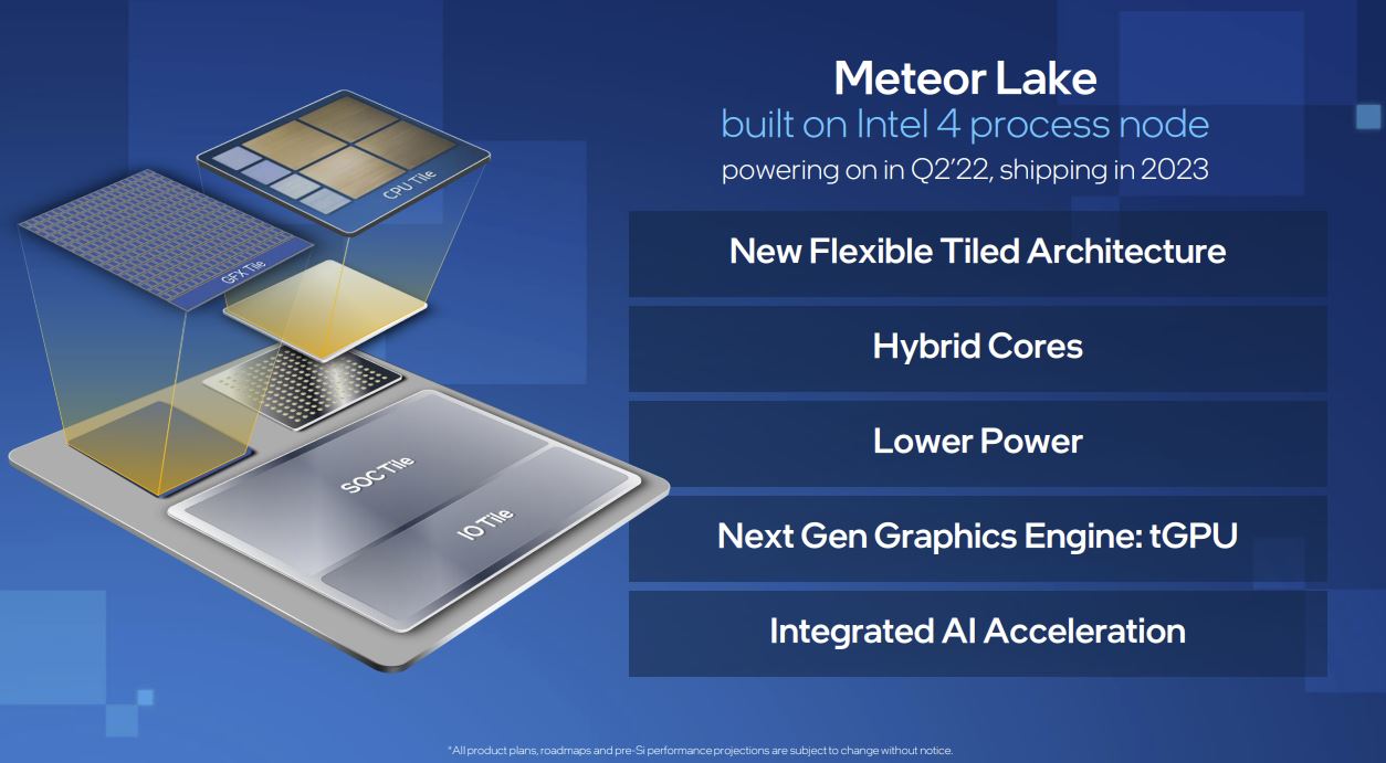
Cost has been one of the overriding concerns with exotic 3D packaging, and Foveros will be Intel's first foray into high-volume manufacturing with its leading-edge packaging tech. However, Intel says that chips produced with 3D Foveros packaging will be extremely price-competitive with standard monolithic (single-die) chip designs — and perhaps even less expensive in some cases.
Intel designed the Foveros die to be as low-cost as possible and still deliver on the company's electrical and performance goals — it's the cheapest die on the Meteor Lake package by orders of magnitude. Intel isn't sharing speeds and feeds for the Foveros interconnect/base tile yet, but says the interfaces can run at 'multiple GHz' in the passive configuration (this statement also heavily implies that Intel has active versions of the interposer already in development). As such, Foveros doesn't incur any bandwidth or latency constraints that require design tradeoffs. Intel also expects the design to scale well in both performance and cost, meaning it can make either value-optimized designs or performance-oriented variants for other segments.
We see the real savings when we zoom out to the bigger picture. Leading-edge nodes are becoming exponentially more expensive per transistor as the industry progresses to smaller nodes, especially with monolithic designs, due to yield concerns. Additionally, designing new IP blocks, like I/O interfaces, for smaller nodes doesn't provide as much of a payoff for the investment. Therefore, re-using non-critical tiles/chiplets on 'good enough' legacy nodes saves time, cost, and developmental resources, not to mention simplifying the testing process.
For a monolithic die, Intel has to serially test the different chip elements, like the memory or PCIe interfaces, which can be a time-consuming process. In contrast, Intel can test chiplets concurrently to save time. Foveros also affords advantages in designing chips for certain TDP ranges, as the different chiplets can be tailored for the needs of the design.
If you think most of these points sound very familiar, you're right — these are the same factors that propelled AMD down the chiplet path back in 2017. AMD wasn't the first to use a chiplet-based design, but it was the first to design a modern mass-produced chip using the design philosophy, so Intel is a bit late to the tech. However, Intel's initial foray with 3D packaging tech is far more complex than AMD's organic interposer-based designs, which will have both advantages and disadvantages. The proof will be in the final silicon, which Intel says is on track for a 2023 launch. Arrow Lake and Lunar Lake will follow in 2024.
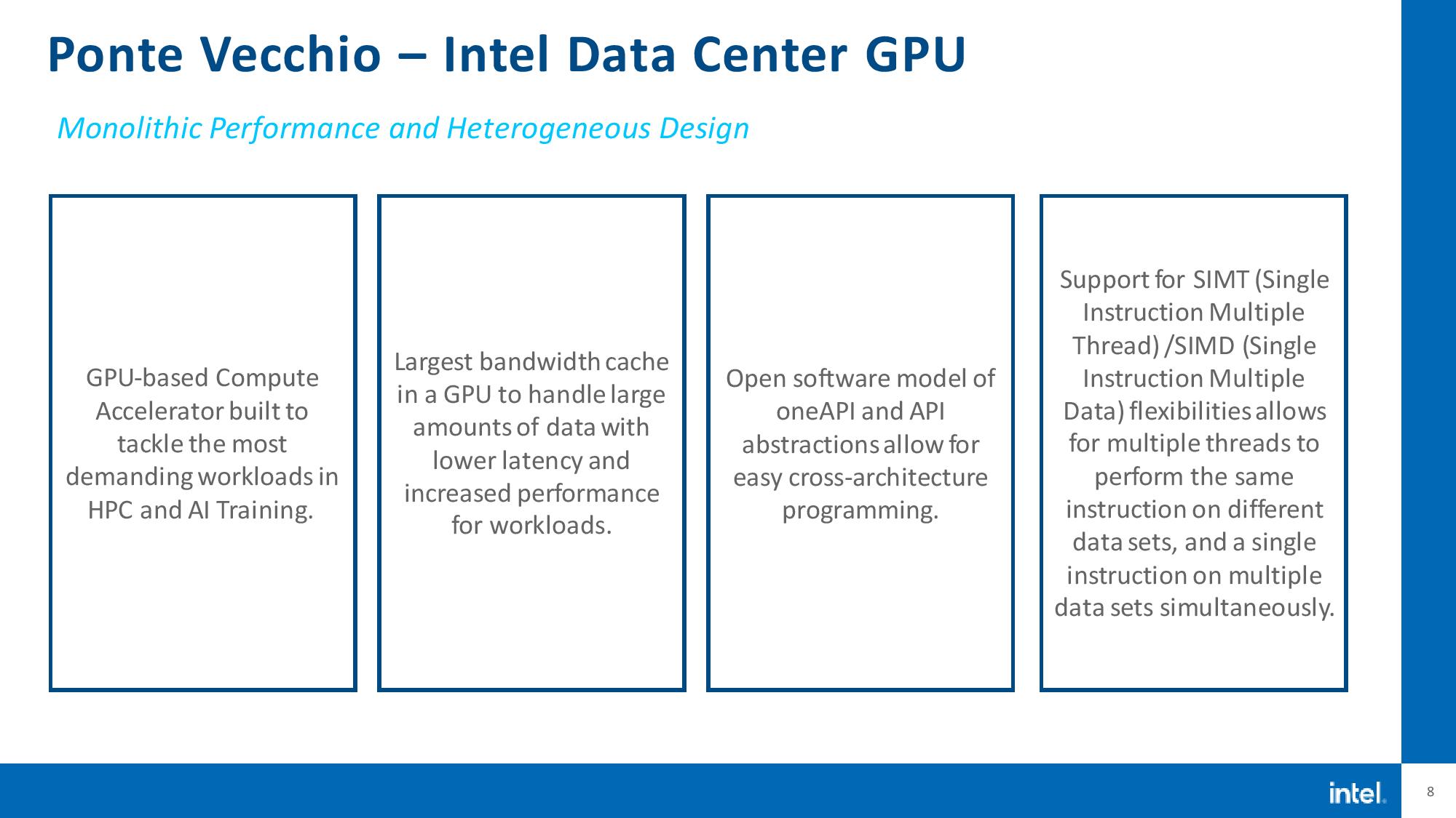
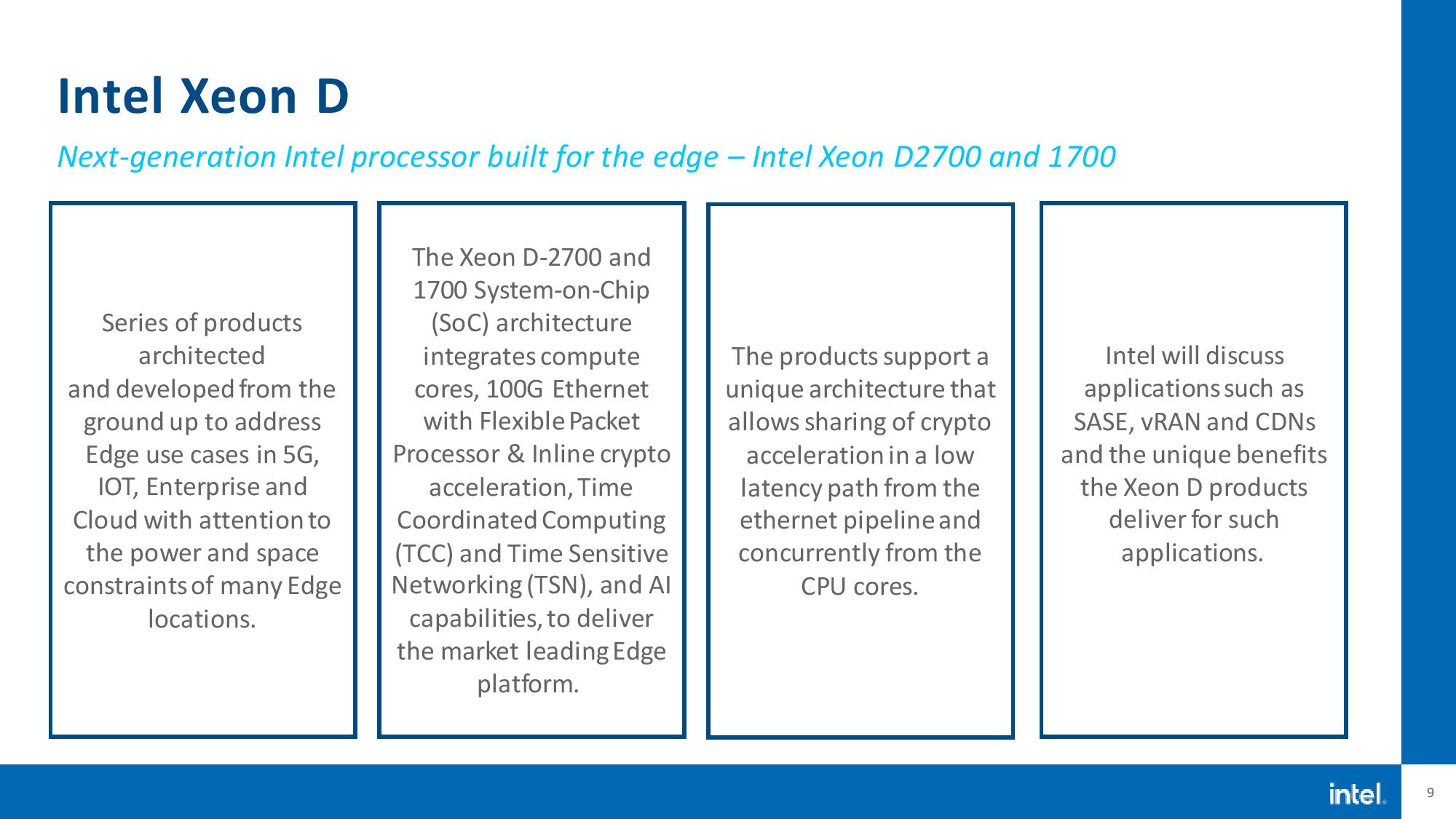
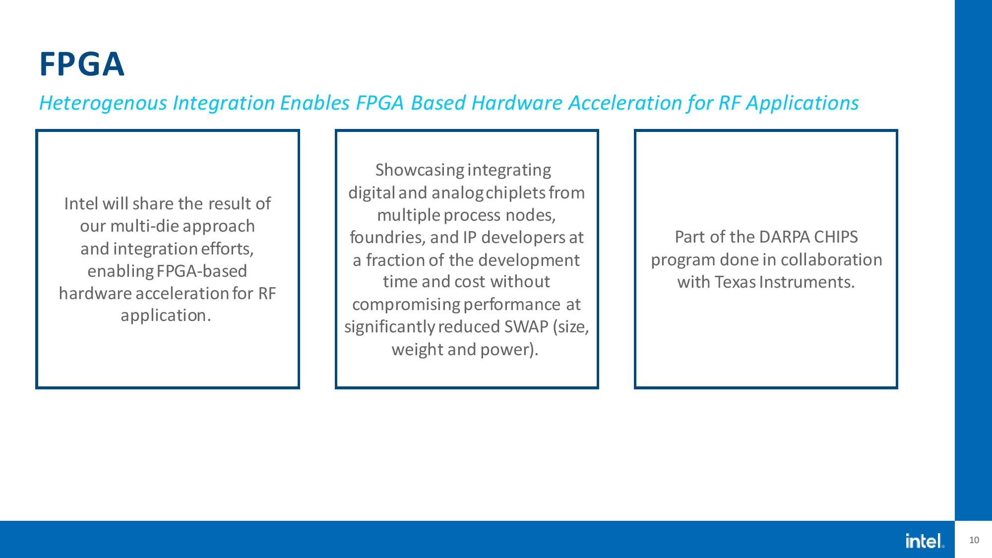
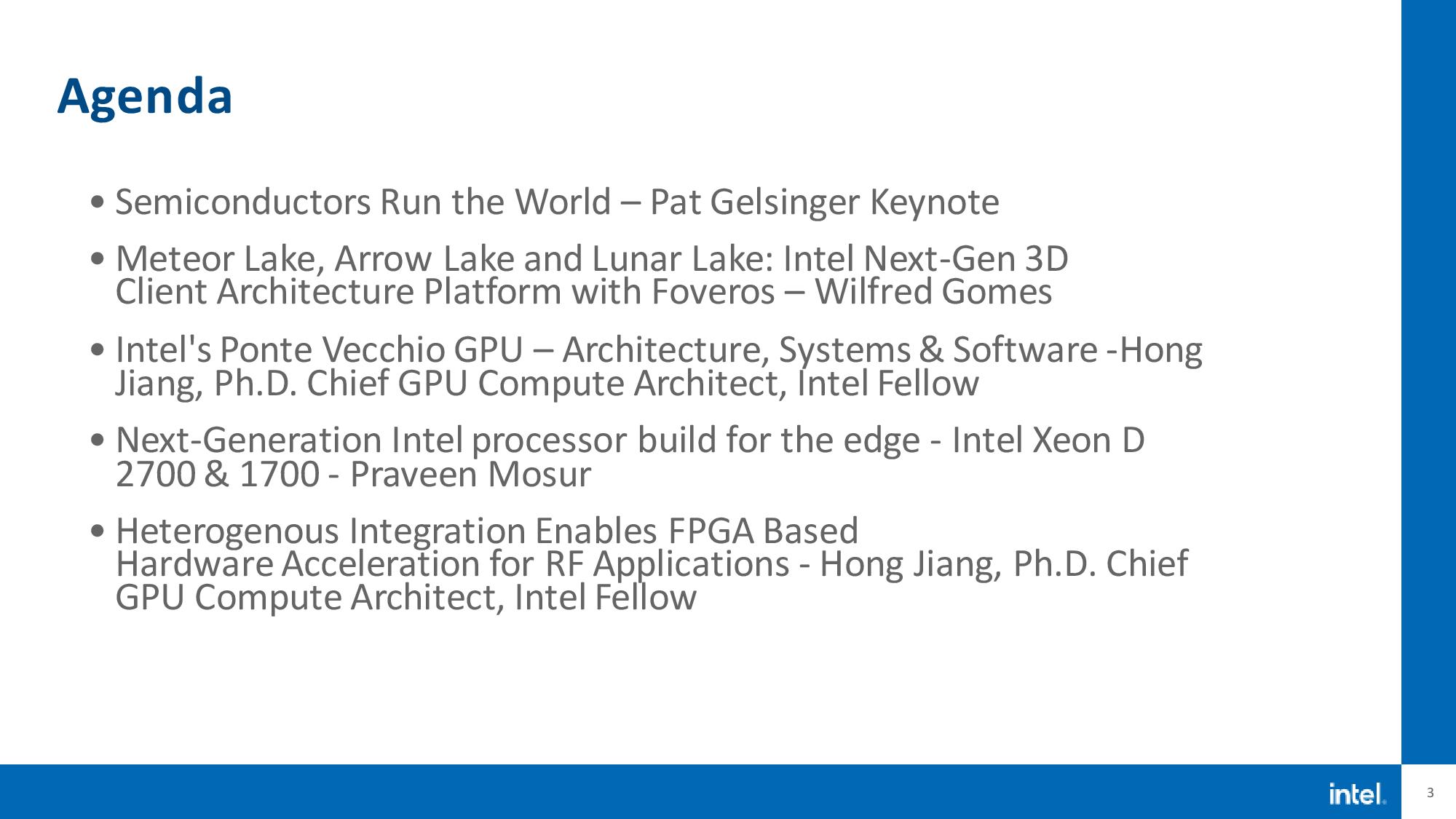
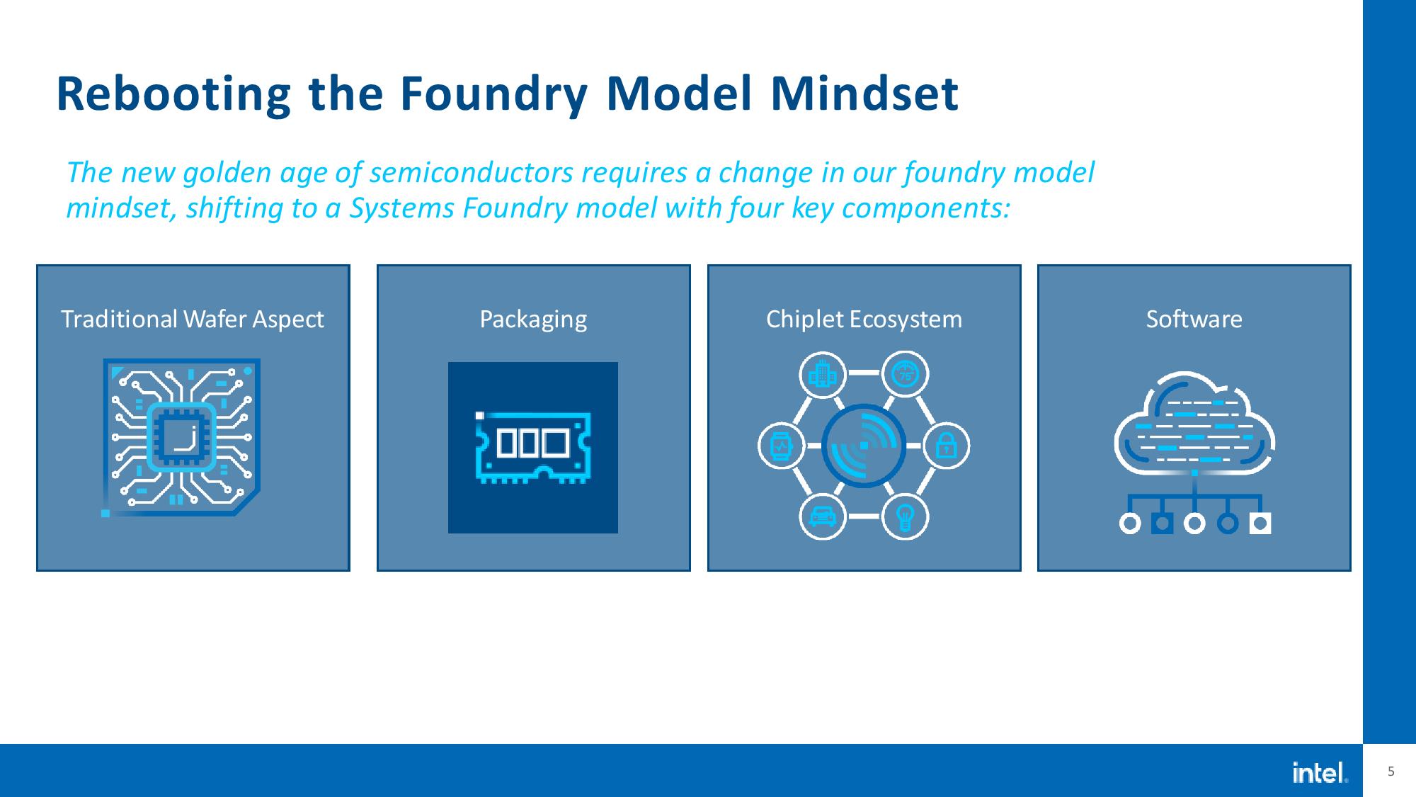
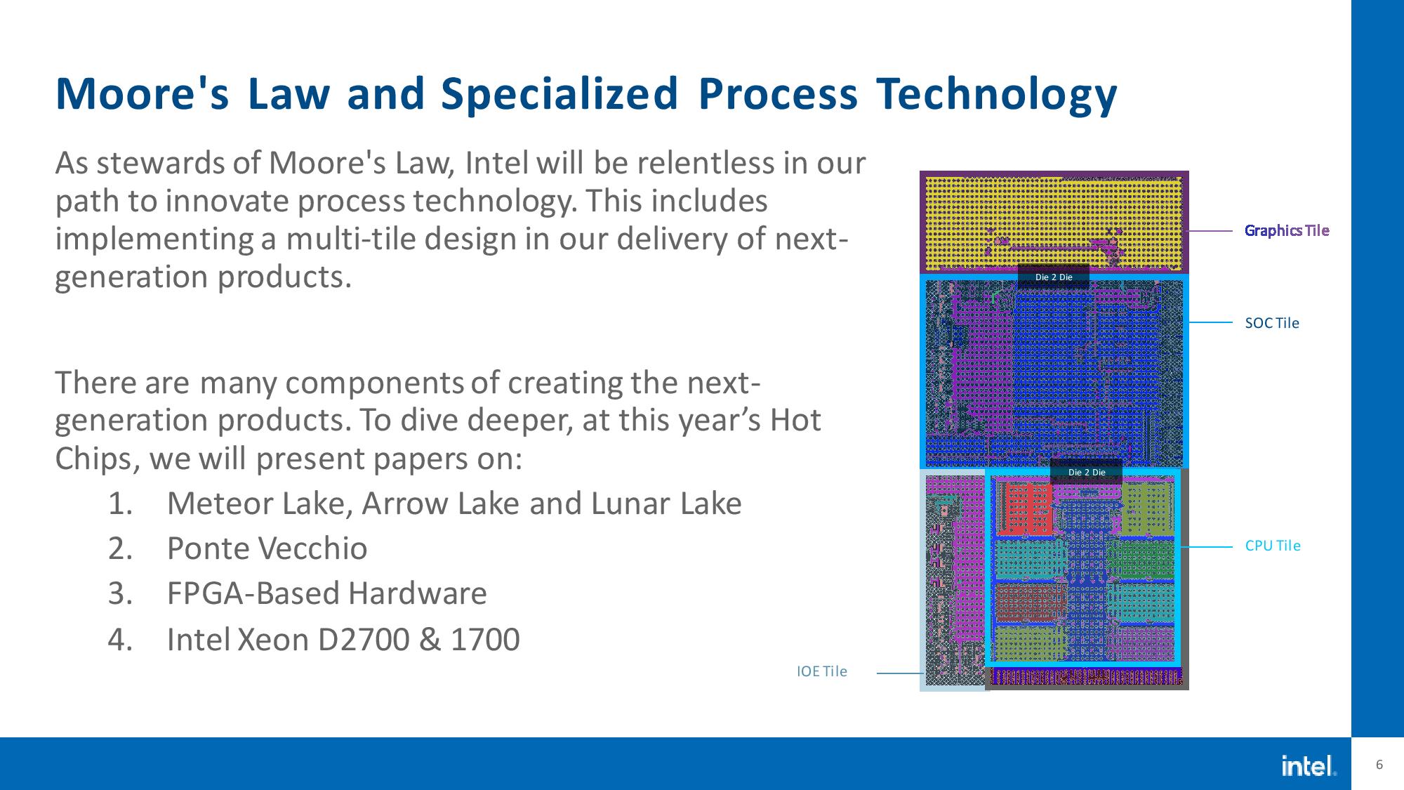
Here's the overview of the topics that Intel will cover this week at Hot Chips 34. We'll have more in-depth coverage as the actual presentations occur, so you can expect an update to this article soon. Stay tuned.

Paul Alcorn is the Editor-in-Chief for Tom's Hardware US. He also writes news and reviews on CPUs, storage, and enterprise hardware.
-
MarioAndLuigiPlumbing ReplyFirst and foremost, there have been recent rumors that Intel's Meteor Lake will be late to market due to Intel switching from the TSMC 3nm node to the 5nm node for its GPU tile/chiplet.
Let's be clear. This chip is 4D, not 3D, as evident by Intel's traveling back in time for their technology. -
jasonf2 So is the magic here that the 3d Foveros acts as a substrate that acts as the fabric interconnect bus and just makes it simpler to arrange chiplets (tiles) in a close package density or are the chiplets themselves stacking? With heat being the biggest limiter won't stacking just amplify thermal issues?Reply -
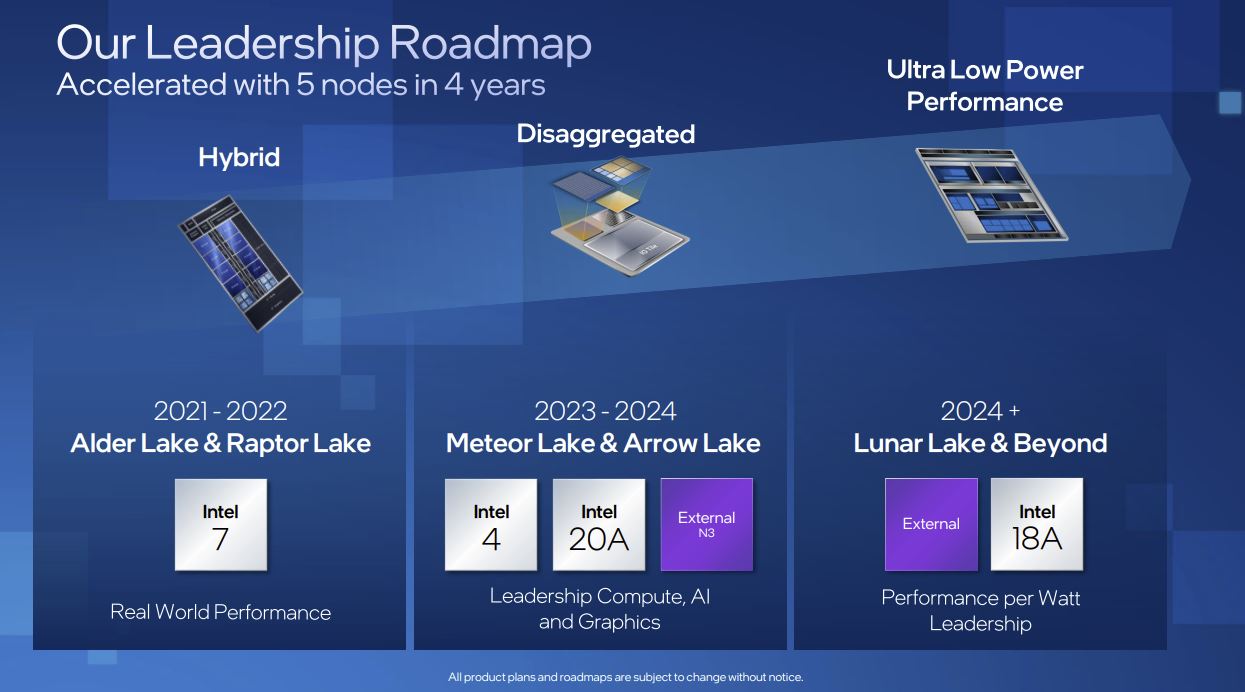
Giroro I think the most telling detail in all of this is the slide that is targeting "2024+" for Performance per watt Leadership. That is the only metric that matters for server and mobile - which is where the money is at.Reply
Intel is basically saying they don't expect to have a competitive product on the market for at least 3 years.
Maybe they'll be able to crank out some 250W+ monstrosity that will get the best gaming performance... but high performance gaming PCs aren't really that big of a market, especially since everybody just upgraded their home PC within the last year or two. -
Johnpombrio As Jason says above, heat is always an issue with chip stacking. I believe the trick is to stack components that do not generate very much heat. Keep the performance cores cool without stacking and stack things like I/O and perhaps memory.Reply -
rluker5 Reply
Looks like the first. Not all that 3d, just grouped on an interposer like vega and hbm. Probably won't be any harder to cool.jasonf2 said:So is the magic here that the 3d Foveros acts as a substrate that acts as the fabric interconnect bus and just makes it simpler to arrange chiplets (tiles) in a close package density or are the chiplets themselves stacking? With heat being the biggest limiter won't stacking just amplify thermal issues?
Hopefully they won't have too much for current limitations. Not that I want to dump 350w into my cpu, I just like to have the option available.
I just thought of my vega comparison. 350w should be fine. -
TerryLaze Reply
That's not even close to being the only metric for servers, having finite space heat and just physical space, how many cores you can fit into a case or how many CPUs you can fit into a single mobo, is just as important.Giroro said:That is the only metric that matters for server and mobile - which is where the money is at.
Then a lot of software charges per cores used so the fewer cores can do the same amount of work is going to be king there.
Then there is hardware support.
Also software support.
And also just availability in large enough numbers that a server would need.
If AMD only wins in perf/watt that is a very small percentage of server customers that want only that and nothing else. -
dalek1234 Replyspongiemaster said:Intel needs to quit releasing details and start releasing products on time.
So true and so sad. Intel talks a big game, but hardly ever walks-the-walk....not for a long time now anyway. -
escksu Replyjasonf2 said:So is the magic here that the 3d Foveros acts as a substrate that acts as the fabric interconnect bus and just makes it simpler to arrange chiplets (tiles) in a close package density or are the chiplets themselves stacking? With heat being the biggest limiter won't stacking just amplify thermal issues?
No, there won't be any heat issue. There is no stacking here at all. It's still all in 2D.
AMD did almost the same thing back in 2015 with Fiji and hbm. The only difference is that Fiji itself is a single die (hbm not part of the GPU) while Intel has 4 separate dies.
Using silicon interposer is obviously a lot more expensive compared to organic one (using the substrate itself). But there are benefits like ability to place the tiles much closer and reduce latency. Having multiple dies also means you need to flatten the surface since there will be minute height variations for each die. More work needed to be done.
Having said that I like this method of puting different dies together. It allows you to use different process and best of all you can go beyond the recticle limit. -
shady28 ReplyTerryLaze said:That's not even close to being the only metric for servers, having finite space heat and just physical space, how many cores you can fit into a case or how many CPUs you can fit into a single mobo, is just as important.
Then a lot of software charges per cores used so the fewer cores can do the same amount of work is going to be king there.
Then there is hardware support.
Also software support.
And also just availability in large enough numbers that a server would need.
If AMD only wins in perf/watt that is a very small percentage of server customers that want only that and nothing else.
That's 100% correct.
To put this in perspective, I'm looking at a bill I pulled up from 2020 on a purchase of 48 core licenses for SQL Server. They charge per core and for outright purchase (not subscription) it's like $160,000 with corporate discount. It looks like it costs about 30% more right now.
In that kind of model, the per-core performance is paramount. If I can get 30% more transactions with core X than with core Y then I need 30% fewer licenses, and that will translate directly into lowering my licensing cost by 30% - which is going to be upwards of $60,000 in the 48 core example above.
And this is just for SQL Server, the OS also charges based on cores. The retail pricing according to Microsoft for Data Center version of of the OS is $6,155 per core.
And Oracle.. jeez. $47,000 per core * a core factor. For Intel/AMD that is $47,000 * .5 = $23,500 per core.
Whoever has the fastest core here wins.