Intel announced the first details of its 'Intel 4' process node and shared an image of a Meteor Lake compute die at the 2022 IEEE VLSI Symposium. Intel claims impressive results with its new 'Intel 4' node over its previous-gen 'Intel 7' node, including 21.5% higher frequencies at the same power, or a 40% power reduction at the same frequency. Intel also claims a 2X area scaling improvement, meaning it has doubled transistor density for the high-performance libraries. The Intel 4 node is also the company's first to use EUV lithography. That's just to name a few among many other notable advancements that we'll cover in more detail below.
Intel's missteps with the 10nm process saw it lose its process tech leadership to TSMC, not to mention cede performance leadership to AMD in the CPU market. As such, all eyes are on the company as its 'Intel 4' process, which we'll refer to as 'I4,' comes to market in 2023.
Intel tried to scale too aggressively with its 10nm node to reach a 2.7X scaling goal. That led to constant delays due to the simultaneous incorporation of multiple new technologies, some of which obviously didn't meet development targets. For I4 and beyond, intel is taking a more modular approach and introducing newer technologies step by step as it progresses to each node, thus delivering a more gradual cadence that it hopes will avoid the delays we've seen in the past.
Intel is developing multiple nodes in parallel to deliver on its promise of five nodes in four years, and I4 is the second step in that journey. First, let's take a closer look at the Meteor Lake die, then dive into the details of the I4 presentation.
Intel Meteor Lake Die Shot


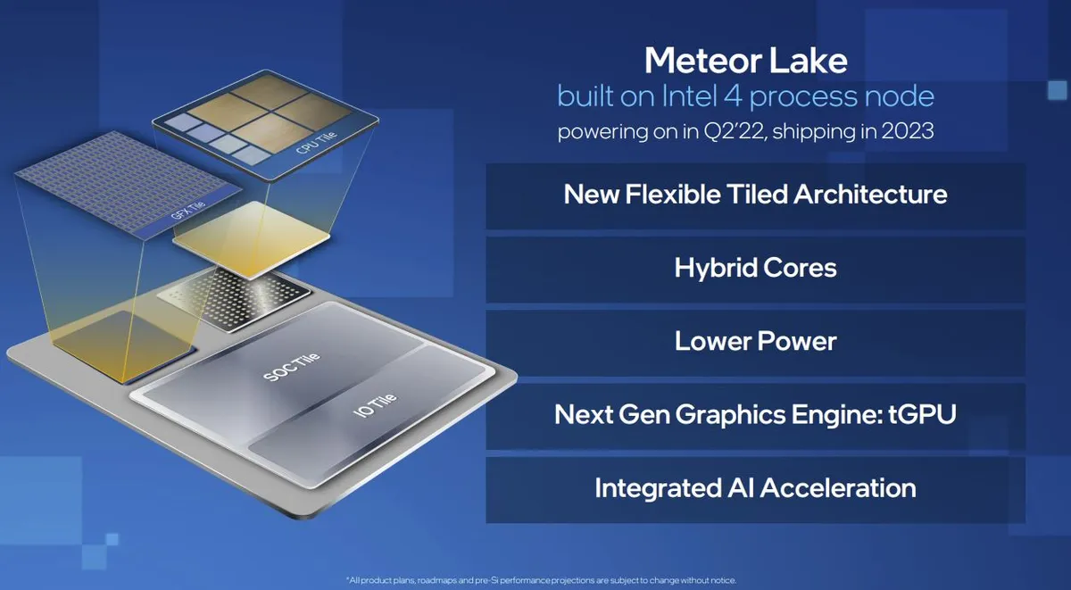
Intel's Meteor Lake will be the first product to market with the I4 process. Intel powered on the compute silicon in April 2022 and claims it has already booted several operating systems. Intel says Meteor Lake is on track for a 2023 launch.
Meteor Lake will use Intel's Foveros 3D packaging tech, just as we saw with the Lakefield processors. However, this will be Intel's first foray into high-volume manufacturing with this leading-edge packaging tech.
Intel will connect the four die (called 'tiles' in Intel parlance) to an interposer through TSV connections. Intel hasn't disclosed if this interposer will be active or passive or if it will hold caches or other control circuitry. Intel will mount four tiles atop this interposer: the compute tile, I/O tile, SOC tile, and graphics tile.
Intel has specified that compute tile will use I4 but hasn't said which nodes it will use for the other tiles. During its Analyst Day earlier this year, the company shared the slide in the above album that lists TSMC's N3 (3nm) node with the Meteor and Arrow Lake processors. This is largely thought to comprise the graphics tile.
As with Alder Lake, the Meteor Lake chips have an x86 hybrid architecture. In this case, we have six p-cores and eight e-cores. The exploded view of the compute die shows us six blue-colored Redwood Cove performance cores (p-cores), used for latency- and performance-sensitive work. We also see two four-core clusters of Crestmont efficiency cores (e-cores) in purple. These cores step in for background and multi-threaded tasks. The center of the chip contains the L3 caches and interconnect circuitry. Intel has yet to provide a further description of the differences between the SoC and I/O tiles, with the former a likely candidate for memory controllers and PCIe interfaces, while the latter could be for Thunderbolt and other PCH-types of interfaces.
Intel isn't giving us much to work with here, but the company shared far more expansive details on the I4 process node that makes the compute die tick.
Intel 4 Process Node

As a quick reminder, Intel recently renamed its process nodes to have a more uniform naming convention that aligns with its primary competitors (third-party foundries TSMC and Samsung). Intel's current flagship process node, Intel 7, used to be called 10nm. Additionally, the I4 node used to be referred to as 7nm. We'll stick with the current naming scheme so there's no (or at least less) confusion.
Intel, like its competitors, usually bakes two versions of each process node — a high-density library that looks to squeeze in the most transistors possible at the expense of performance, and a high-performance library that trades off some transistor density to provide more performance. Naturally, Intel and its competitors always refer to the high-density library for the density metrics they use for marketing. Still, most of the flagship high-performance chips you see on the market actually use the less-dense library.
Quite surprisingly, Intel isn't creating a high-density library for its I4 node; instead, it will focus solely on high-performance products for I4. Intel says that I4's successor, 'Intel 3,' will come with both high-performance and high-density libraries. Notably, Intel recently announced that it would delay its Granite Rapids Xeons from 2023 to 2024 due to switching the design from I4 to 'Intel 3' (I3).
The I4 node is forward compatible with I3, so designs can be moved between the two without going through the usual time-consuming steps of porting an architecture. The I3 process will also have enhanced transistors and interconnects, along with more EUV layers to further simplify the design. The I3 node will be 18% faster than I4 and will be the first new node Intel will offer its customers through Intel Foundry Services (IFS) (the company already offers its existing 16nm).
After I3, Intel will move to the angstrom era with the 20A and 18A nodes, both of which will introduce even more exotic new tech, like new RibbonFETs (gate all around/nanosheet) and PowerVia (backside power delivery) tech.
| Row 0 - Cell 0 | Intel 4 | Intel 7 | TSMC N5 | TSMC N3 |
| HP Library Density | 160 MTr/mm^2 (est.) | 80 MTr/mm^2 | 130 MTr/mm^2 (est.) | 208 MTr/mm^2 (est.) |
| HD Library Density | None Planned | 100 MTr/mm^2 | 167 MTr/mm^2 (est.) | 267 MTr/mm^2 (est.) |
| Logic Density | 2x | 2.7x | 1.83x | 1.6x |
| Perf (iso power) | 1.2X | 1.15x | 1.15x | 1.11x |
Intel isn't sharing specific transistor density metrics yet, instead giving us a basic claim of 2X scaling (much more on that topic below). However, the company says it will share an MTr/mm^2 (mega-transistor per squared millimeter) transistor density metric in the future, and that I4's transistor density generally tracks with the 2x area scaling. As such, we use an extrapolated transistor density in the above table (source). These numbers are estimates, but it appears that I4's density will land between TSMC's high-performance N5 and N3 libraries.


Intel 4 (I4) promises a 21.5% improvement in frequency at the same power as the previous-gen I7 process, or 40% less power. As mentioned, Intel claims a 2x area scaling improvement over I7, which comes as the culmination of several technologies.
The I4 node is Intel's first node to extensively use EUV lithography to simplify manufacturing, and we can see the results in the second and third slides in the above album. Intel's previous-gen process requires multiple immersion lithography steps to process some layers of the stack, but EUV allows the company to use one exposure to etch a single pattern. This reduces the number of steps in the process flow by 3 to 5x for that portion of manufacturing.
Naturally, EUV results in fewer defects, thus providing higher yields. It also increases processing speed significantly, but it has other benefits, too. For example, the underlying metal stack must also be aligned at each step in the manufacturing flow. Thus, EUV helps with yield issues that occur due to misalignments because the layers only have to be aligned once for that section of the manufacturing flow rather than multiple times. This further improves yield.
Intel uses EUV in both the front and back end of the manufacturing flow. As seen in the third slide, the result is that I4 has 5% fewer process steps and a 20% lower total mask count than I7. As you can see by the extrapolated result in the center of the charts, without EUV, I4 would require more steps than I7. Unfortunately, Intel hasn't divulged the exact number of layers it etches with EUV lithography.
Intel's Contact-Over-Active-Gate (COAG) debuted with the I7 process and increased density by moving the contact from the edge/outside of the gates and placing it on top of the gates. The second generation of this tech helps to further improve density in the I4 process. Likewise, Intel removed dummy gates from I7 but improved that technique with I4 by removing a diffusion grid between the arrays. Intel also went from four fins to three.
The I4 node has 18 metal layers compared to the I7 node's 17 metal layers, with enhanced copper introduced into the lower metal layers to improve electromigration/reliability while maintaining performance (more on that below). We also see reduced pitch throughout the entire stack. (The two thick metal layers are for power routing.)


Power, Performance, and Area (PPA) are where the rubber meets the road. Here we can see the slides that claim a 21.5% performance improvement at the same (ISO) power over I7, or 40% better power at the bottom of the frequency/voltage curve. This is due to tuning for both the upper and lower voltage ranges, ultimately resulting in a better dynamic range throughout.
The I4 process has two different types of SRAM cells. It's well known that SRAM doesn't scale as fast as logic. Intel has disclosed a .77x scaling for its High Density Cell (HDC) but hasn't disclosed the scaling metric for the High Current Cell (HCC).
Interconnects, the tiny wires that connect transistors, continue to become smaller over time, now only being the width of a few electrons. As such, they've become one of the main barriers to increasing transistor density, as smaller transistors simply require smaller wires. Intel switched to using cobalt instead of copper with its I7 process node, resulting in less performance. It was also rumored to be part of the reason for the incessant delays that cost the company its leadership position.
Intel disclosed that it uses enhanced copper in the M0 to M4 layers to improve interconnect performance and shared slides (second and third in the above album) that show the improvements it has made in the critical lower layers. Here we can see two of these approaches with the I7 node — one with pure cobalt with a tantalum barrier, and another with a tantalum nitride barrier over copper alloy. These two approaches each have significant tradeoffs for either resistance (performance) or reliability (electromigration).
The I4 process uses an 'enhanced copper' design that leverages a tantalum barrier with cobalt cladding over pure copper. This design provides the best of both performance and reliability.
Finally, Intel divulged that it has doubled its MIM capacitance density over the I7 process. As a reminder, this is the Metal-Insulator-Metal (MIM) capacitor that Intel branded as 'SuperMIM" with the then-10nm process. This helps combat Vdroop, which helps ensure longer sustained frequency potential by eliminating localized chip brownouts during power-intensive work, like SIMD instructions. As a result, sustained clock speeds should improve dramatically.
Intel's Hillsboro facility will be the first to produce I4 devices, and the Ireland campus is the obvious next candidate due to the fact that it is the only other known Intel campus with an EUV machine. We'll learn more about Intel 4 as it comes closer to market in Meteor Lake, which Intel says arrives on the market in 2023.
