Microsoft's CPU/GPU Combo Chip is Called 'Vejle'
Microsoft and IBM beat Intel and AMD in designing a CPU and GPU combo chip.
Get Tom's Hardware's best news and in-depth reviews, straight to your inbox.
You are now subscribed
Your newsletter sign-up was successful
We've been waiting for the realization of all the talk about the combination of CPU and GPU into a single chip for some time now. AMD and Intel will be achieving that goal in the not too distant future, but a major software giant (along with some other hardware help) beat them to the punch.
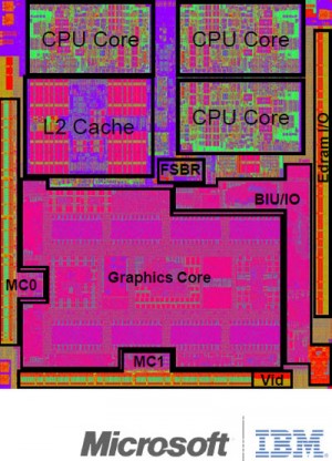
Microsoft's latest redesign of the Xbox 360 houses a CPU and GPU combo chip, which includes IBM's triple-core design with ATI's graphics core, and is called Vejle, named after a city in Denmark (not Valhalla, as many previously believed).
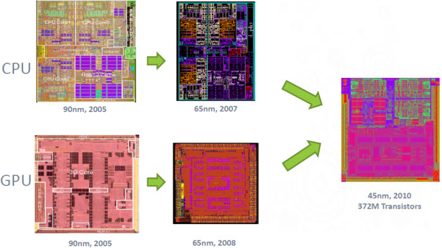
The two parts originally debuted as 90nm parts (codenamed Xenon for the IBM CPU and Xenos for the ATI GPU) but are now married as one 45nm part produced by IBM and Globalfoundries.
Compared to the original duo of chips, this single SoC is 50 percent smaller in size and draws 60 percent less power. This clearly reduces cost for Microsoft in both silicon as well as design of cooling hardware.
Despite being the first of its kind on such a mass scale, the new Vejle chip contains only 372 million transistors, which is about half as many as the Core i5-760.
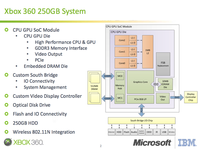
Despite the fact that the CPU still runs at 3.2GHz and the GPU at 500MHz, the overall design is capable of higher performance than the original design thanks to its integrated design. Sadly, instead of the new Xbox 360s being able to take advantage of the improvements, the system must be throttled to maintain compatibility with the previous designs.
Seen in the block diagram is the FSB replacement, which puts limits the latency and bandwidth on the new chip so that it'll behave the same way as the older chips.
Get Tom's Hardware's best news and in-depth reviews, straight to your inbox.
(Sources: Ars Technica, Venture Beat.)
-
Darkerson Thats pretty sad that game console tech more or less one upped pc tech, but good for them I guess.Reply -
warezme If it were a PC it would get unlocked, overclocked and better cooling put on the thing to make it better.Reply -
nforce4max Nice work, it is a shame about the throttling. This is why consoles usually never live up to their true potential and they often cut corners by reducing costs and in this case the cooling system. They should have put much more memory in this console. The more memory the better the games that devs can make graphics wise as well content.Reply -
counselmancl the overall design is capable of higher performance than the original design thanks to its integrated designReply
Who designed this? -
werfu Why throttle it? Its been years since programmer last used the CPU frequency to time their game. Having it run full potential would simply let the CPU idle more often and reduce game lag under intense sequence.Reply -
smeker DarkersonThats pretty sad that game console tech more or less one upped pc tech, but good for them I guess.Reply
How exactly did game console tech upped the pc tech?
What the person that wrote this article dont understand is that MS is using a four year old architecture of a 3 core cpu. They just shrunk the size and placed it on a single silicone. Instead of using 90nm they used 45 nm tech to print the CPU and GPU on a single silicon. You can see that from the images above.
Why dont they try doing that with an i5 CPU and and hd 5870 or GT480...
There is nothing revolutionary in this chip.... -
siman "Microsoft and IBM beat Intel and AMD in designing a CPU and GPU combo chip."Reply
umm ATI is AMD....or DAAMIT... -
rocket_sauce werfuWhy throttle it?My guess would be to avoid the fiasco of the dreaded RROD of its last gen predecessor and to keep cooling on the cheap side.Reply
smekerHow exactly did game console tech upped the pc tech?Sounds to me he is just talking about a console getting this tech before a PC.


