
On Wednesday, Intel announced that Fab 9 had begun operations at its Rio Rancho site in New Mexico. The $3.5 billion production facility was built to package chips using Foveros 3D technology and is one of Intel's first fabs dedicated solely to advanced packaging technologies.
"Today, we celebrate the opening of Intel's first high-volume semiconductor operations and the only U.S. factory producing the world's most advanced packaging solutions at scale," said Keyvan Esfarjani, Intel executive vice president and chief global operations officer. "This cutting-edge technology sets Intel apart and gives our customers real advantages in performance, form factor and flexibility in design applications, all within a resilient supply chain. Congratulations to the New Mexico team, the entire Intel family, our suppliers, and contractor partners who collaborate and relentlessly push the boundaries of packaging innovation."
Article continues below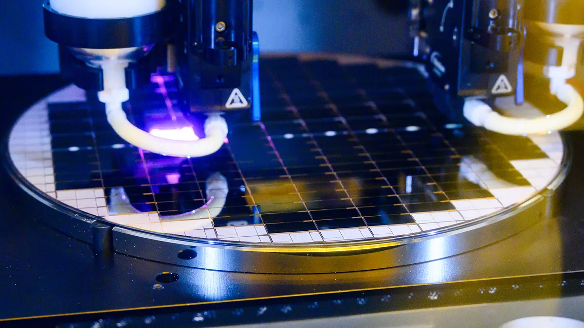
The current iteration of Intel's Foveros 3D relies on a 600mm^2 interposer produced using its low-cost and low-power22FFL process technology that acts like an interconnect and a power delivery base die for chiplets that are stacked on it. For now, Foveros 3D features 36-micron bump pitches and supports up to 770 microbumps per square millimeter and up to 160 GB/s per mm bandwidth. However, the technology will adopt 25-micron and 18-micron micro bumps in the future, drastically improving interconnection densities. Furthermore, multiple Foveros 3D interposers can be interconnected using Intel's Co-EMIB technology to build ultra-large datacenter-grade devices.
Building an advanced packaging facility in New Mexico is an essential step in Intel's broader strategy to increase the production of advanced semiconductor products in the U.S. In addition to Fab 9, the company is constructing multiple leading-edge fabs in Arizona and Ohio.
"This investment by Intel underscores New Mexico's continued dedication to bring manufacturing back home to America," said Government Michelle Lujan Grisham. "Intel continues to play a key role in the state's technology landscape and strengthen our workforce, supporting thousands of New Mexico families."
