Samsung extends LPDDR5 to 12.7 GT/s: Next-gen devices enjoy a nice speed boost
Samsung's LPDDR5-Ultra-Pro further clings into LPDDR6 territory

Samsung has introduced yet another extension to the LPDDR5 specification at the International Solid-State Circuits Conference (ISSCC), increasing data transfer rates to 12,700 MT/s (12.7 GT/s). To increase the speed, Samsung had to add four-phase self-calibration and AC-coupled transceiver equalization to its DRAM chips, which it calls its LPDDR5-Ultra-Pro DRAM.
World's fastest LPDDR5X
Samsung's highest-speed LPDDR5X, with a data transfer rate of 12,700 MT/s, is a 16 Gb memory IC with an industry-standard voltage of 1.05V made using the company's 5th Generation 10nm-class DRAM fabrication process. 16 Gb device capacity may not be too impressive on the mobile devices front, considering Samsung announced 24 Gb LPDDR5X ICs in 2023 and then launched 32Gb LPDDR5X ICs in 2024. However, 16 Gb could be quite a decent capacity for applications that do not demand the highest memory densities. This is perhaps why Samsung's ISSCC paper mentions AI, AR, VR, and server applications, whereas the company's presentation mentions LPCAMM2 modules aimed at PCs and servers (well, edge servers).
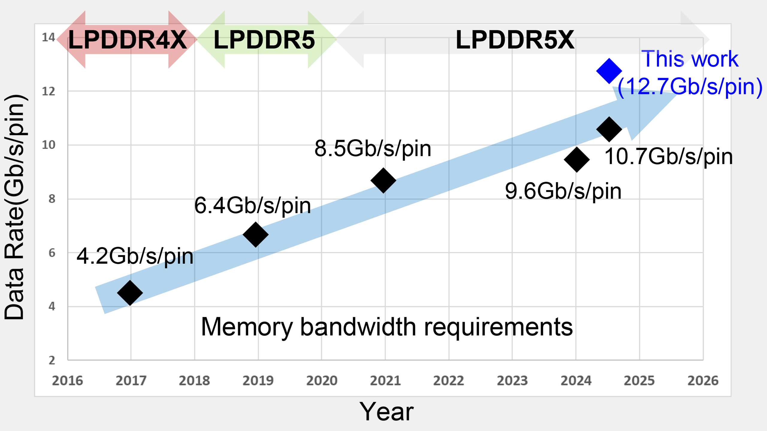
The LPDDR5 specification was introduced in 2019 with the plan to extend the data transfer rate to 6,400 MT/s. In 2021, JEDEC published an extended version of the spec — dubbed LPDDR5X — that pushed the speed to 8,533 MT/s. But that was not enough for at least some LPDDR5X users, so Micron, Samsung, and SK hynix further increased the data transfer rate of LPDDR5X to 9,600 MT/s in 2023, and then Samsung followed up with 10,700 MT/s in 2024 (which it has yet to ship). Now, Samsung has taken another step and introduced LPDDR5-Ultra-Pro memory with a 12,700 MT/s data transfer rate.
Enabling such an extreme data transfer rate required Samsung to implement a four-phase self-calibration loop and AC-coupled transceiver equalization. These two features are not defined in the LPDDR5X specification and are vendor-specific circuit-level design techniques used to meet or exceed the official JEDEC LPDDR5X data rate and power requirements.
Four-phase self-calibration loop
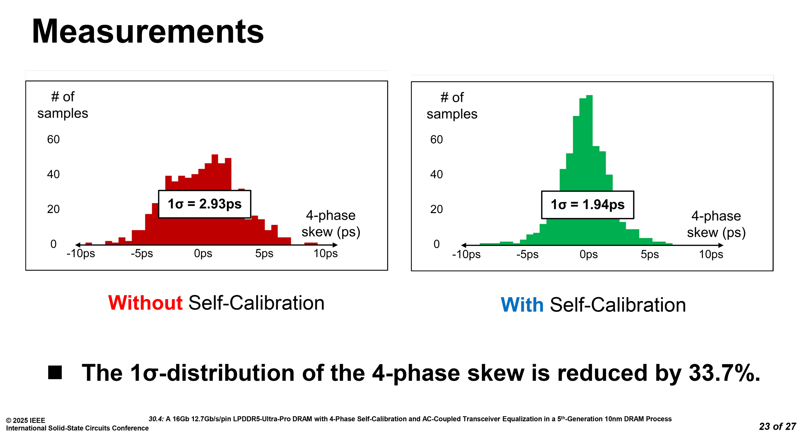
A four-phase self-calibration loop is a circuit-based solution that ensures four internal clock phases (0°, 90°, 180°, and 270°) remain properly aligned in high-speed memory interfaces. In LPDDR5X DRAM, clock signals are divided and distributed to create these four phases, which drive data transfers at multi-GT/s speeds. Even slight mismatches between these phases — called phase skew — can affect the timing margin and degrade performance. The calibration loop measures each pair of phases (e.g., 0° vs. 180°, 90° vs. 270°) and automatically compensates for any offset.
Samsung's implementation of the four-phase self-calibration loop uses two calibration steps: flip and unflip. By flipping which signal is fed to the circuit under test (e.g., swapping 0° and 180°) and comparing the results against the unflipped measurement, the calibration logic isolates and corrects the true clock-phase misalignment. The final calibration codes are then applied to shift or adjust each phase as needed to preserve clean, evenly spaced clock edges inside the chip.
AC-coupled transceiver equalization
At high-speed data transmission rates, signals are prone to attenuation and inter-symbol interference (ISI) along the channel. AC-coupled transceiver equalization addresses signal issues in high-speed DRAM components: on a high level, it boosts the clock signal, equalizes the receiver, and pre-emphasizes the transmitter.
Get Tom's Hardware's best news and in-depth reviews, straight to your inbox.
Samsung's implementation involves three complementary blocks: an AC-coupled booster (ACCB) in the clock buffer, an AC-coupled equalizer (ACCE) on the receive side, and an AC-coupled pre-emphasis (ACCP) on the transmit side. Each applies extra high-frequency gain at various points in the path, ensuring that attenuated clock edges are restored and timing integrity is maintained. According to Samsung, the net effect is more robust data transmission and reception at speeds exceeding 10,000 MT/s per pin.
Measurements


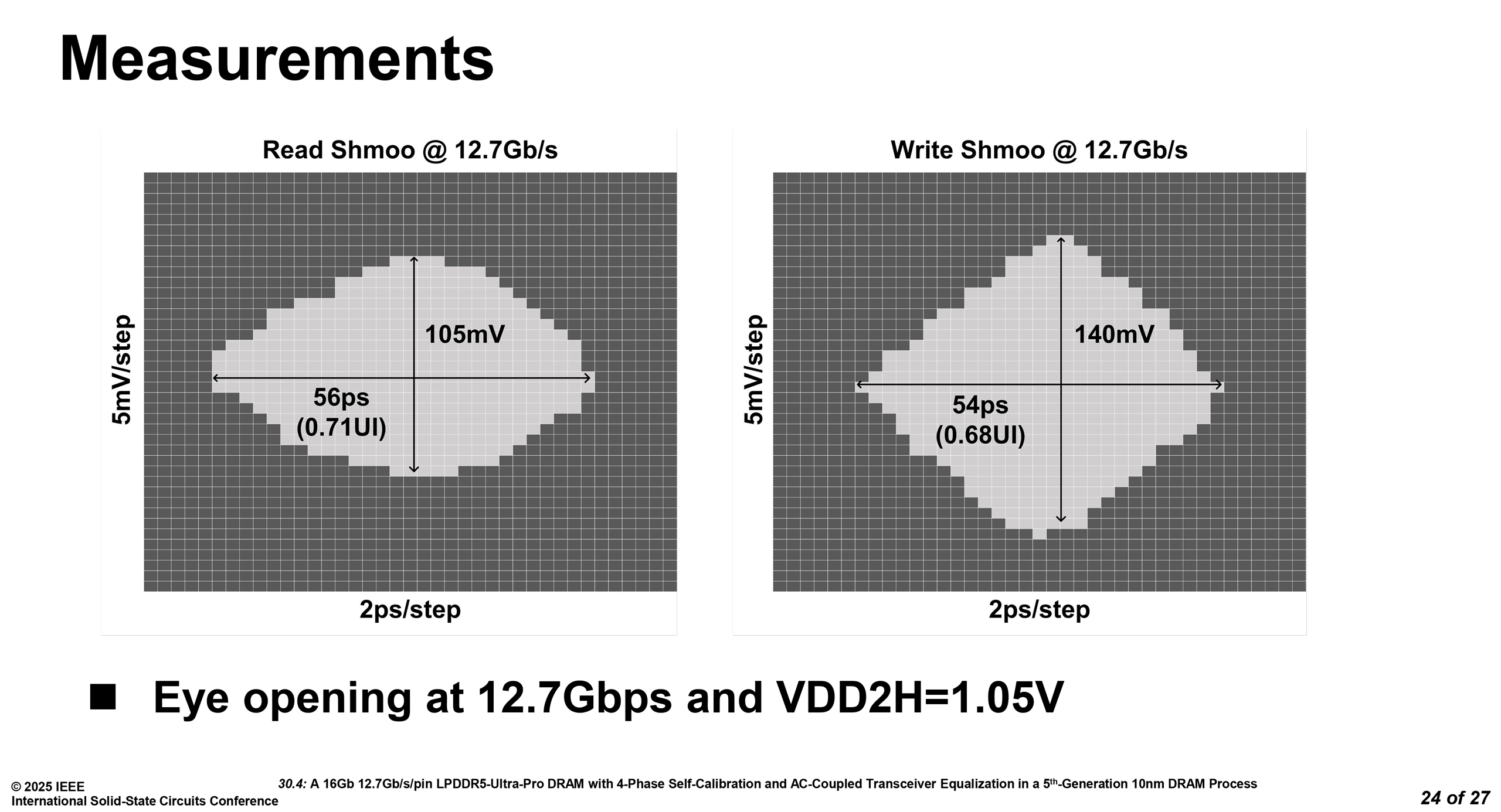
Based on the company's own measurements, at its maximum rate of 12,700 MT/s, Samsung's LPDDR5-Ultra-Pro DRAM memory chip operates reliably at 1.05 volts. Even at 10,700 MT/s, it maintains stability above 0.9 volts, according to measurements conducted by Samsung. The read and write margins at peak speed measure 0.71 and 0.68 unit intervals, respectively, demonstrating robust signal integrity. These values confirm the effectiveness of Samsung's calibration and equalization techniques.

Anton Shilov is a contributing writer at Tom’s Hardware. Over the past couple of decades, he has covered everything from CPUs and GPUs to supercomputers and from modern process technologies and latest fab tools to high-tech industry trends.
-
bit_user Cool. So, at 128 bits, that'd be a nominal data rate of 203.2 MB/s?Reply
Also...
What's "Shmoo"?
: D
Lastly, is LPDDR5 memory stackable? I sort of assumed it must be, or else I don't see how they can possibly fit so much on package. If so, is it all stackable or just specific dies? -
usertests Are there some benefits to avoiding moving to LPDDR6? Maybe less complexity and initial cost-per-bit?Reply -
bit_user Reply
First, is the spec even finalized?usertests said:Are there some benefits to avoiding moving to LPDDR6? Maybe less complexity and initial cost-per-bit?
Second, CPU makers and DRAM makers need to synchronize their launch of products supporting it. So, by releasing faster LPDDR5X, Samsung is possibly getting out ahead of the LPDDR6 transition and perhaps helping CPU makers to do the same.
There are also possibly interesting implications for AI and some server applications. For instance, Nvidia opted to use LPDDR5 with their Grace CPUs, because they said it was 1/3rd the cost of HBM and I think also lower power per bit. I expect their Digits device is using LPDDR5X, as well. Finally, they have that new SOCAMM standard they're working on, and presumably that would use LPDDR5X. -
Notton Slap this RAM onto a Ryzen 395+ (Strix halo) and, assuming it works, the memory bandwidth hits 406GB/s.Reply
That will easily surpass a RX7600 at 288GB/s, and nip at the heels of a RX7700 at 432GB/s.
Apple M4 Max 14-core hits 410GB/s, while the 16-core version hits 526GB/s.
That is properly fast, and sounds justifiable in a $2800 tablet. -
bit_user Reply
By my calculations, the GPU of the Ryzen 395+ is close to that of the PS5, which has a memory bandwidth of 448 GB/s. Furthermore, although it's higher than regular DDR5, I'd bet the latency of LPDDR5X is lower than GDDR6 and we know games tend to be rather sensitive to memory latency.Notton said:Slap this RAM onto a Ryzen 395+ (Strix halo) and, assuming it works, the memory bandwidth hits 406GB/s.
That will easily surpass a RX7600 at 288GB/s, and nip at the heels of a RX7700 at 432GB/s.