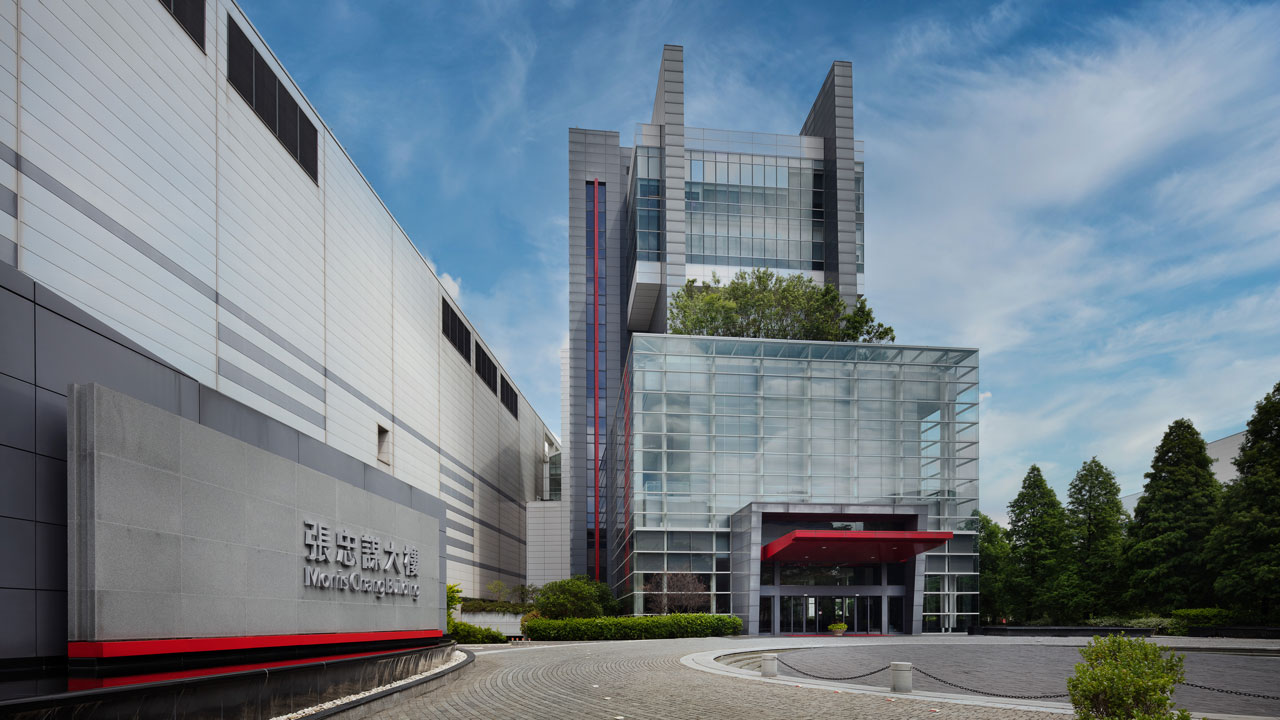
TSMC to open Japan's most advanced semiconductor production facility in February - chip production begins in H2
The plant will initially produce 28nm class technologies.

TSMC will host a formal opening ceremony for its first fab in Japan on February 24, 2024, new reports say. The semiconductor production facility will be capable of making chips using TSMC's N28 (28nm-class) technologies -- and will be the most advanced logic fab in the Land of the Rising Sun.
TSMC's Japanese fab will be located near Kumamoto, a city on the Japanese island of Kyushu, China Times reports citing Japanese media sources. The semiconductor manufacturing facility is set to process wafers using a variety of production nodes derived from the company's N28 (28nm-class) technology. This includes several N28 variants and the 22ULP fabrication process, a specialty node for ultra-low-power applications. While these manufacturing technologies are too outdated for use in advanced system-on-chips (SoCs) for smartphones or PCs, not to mention high-performance CPUs or GPUs, they are adequately suited for components used in the automotive and consumer electronics sectors. There remains a lot of demand for such processors in Japan with its multitude of sizable companies operating in these sectors.
These technologies are expected to remain relevant for an extended period, given the long lifecycle of many integrated circuits (ICs). TSMC now plans to host a formal opening ceremony on February 24 and the fab will start producing chips in the second half of 2024, as planned. It is rumored that eventually, TSMC will build another fab in Japan that will be capable of processing wafers using TSMC's N16-derived process technologies, which include N16, N12, and N12e, which belong to 16nm and 12nm classes.
The fab will employ approximately 1,700 people when fully operational. Currently, the facility has about 1,400 employees and 250 new graduates are expected to join in the spring of 2024, according to China Times.
TSMC — the world's No.1 contract maker of chips — is expanding its operations beyond Taiwan, driven both by a surge in chip demand and influenced by the current geopolitical landscape. In Japan, the company is building up its fab in collaboration with Sony. The monthly production capacity of the fab near Kumamoto is set to be 45,000 wafer starts per month and the initial investment in the fab was set to be $7 billion, with the Japanese government subsidizing the project. The final cost is unknown though.
TSMC is also in the process of setting up a research and development center in Japan and is engaged in various collaborative projects with the University of Tokyo.
Get Tom's Hardware's best news and in-depth reviews, straight to your inbox.

Anton Shilov is a contributing writer at Tom’s Hardware. Over the past couple of decades, he has covered everything from CPUs and GPUs to supercomputers and from modern process technologies and latest fab tools to high-tech industry trends.
-
Co BIY Replythisisaname said:Japan that far behind🤯
Everyone is that far behind because there are only three leading edge fab companies.
TSMC is finally becoming a multi-national corp rather than simply a global one. -
usertests Reply
I'm still using a GPU made on a 28nm process. 🫠thisisaname said:Japan that far behind🤯 -
TechLurker Ever since CRADA denied Japan licensing rights to EUV tech, Japan lost the lead in the 90s. Now, it's indirectly coming around full circle with a Japanese TSMC branch and access to fairly modern EUV machines.Reply
I suspect part of this also helps with negotiating more access to the valuable chip manufacturing chemicals that Japan has a borderline monopoly on. -
Joseph_138 High tech companies need to leave the far East, before China swallows them up, and steals all of their technology.Reply