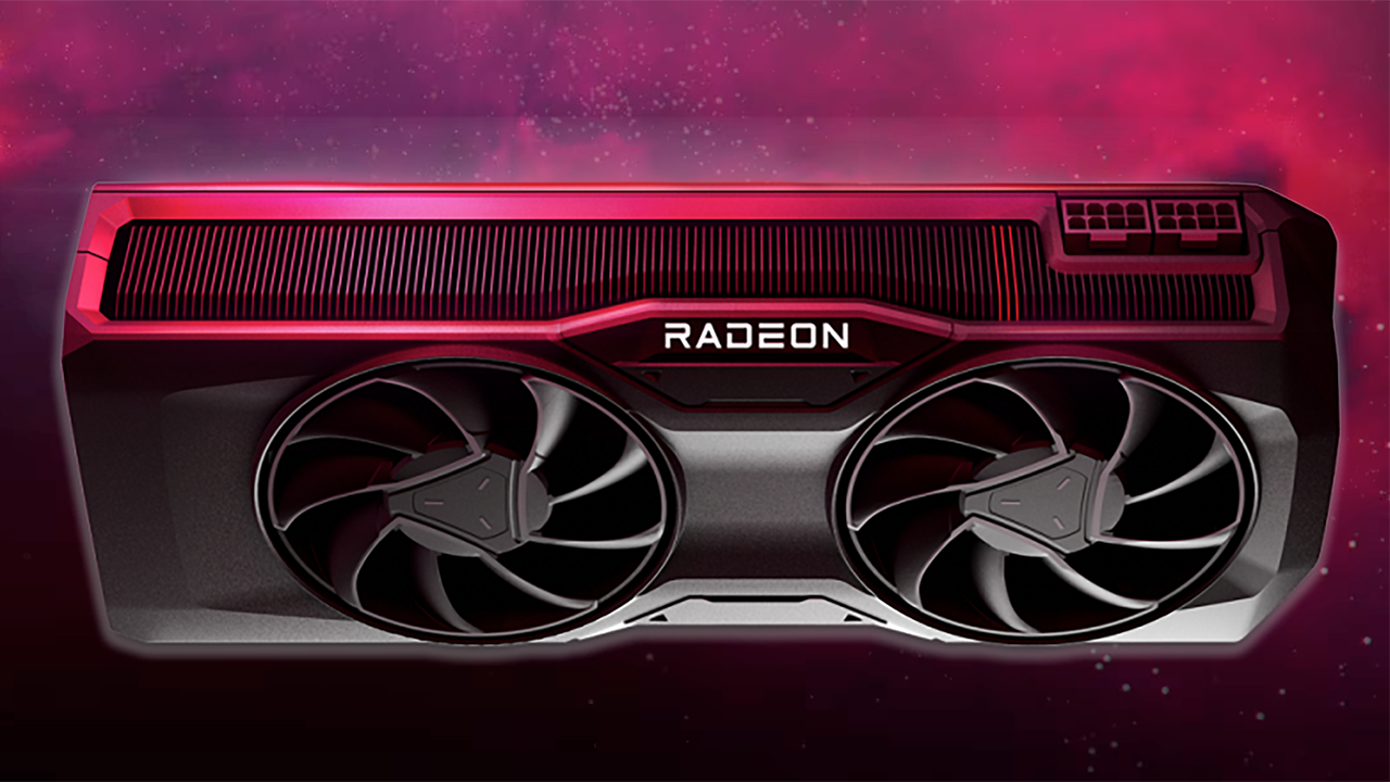
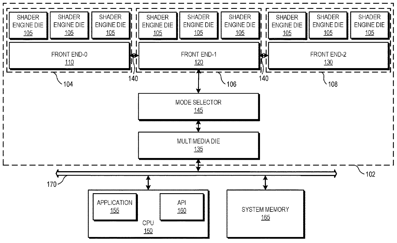
AMD patents configurable multi-chiplet GPU — illustration shows three dies
AMD looking to further optimize GPU designs.

Splitting complex chip designs into multi-chiplet solutions is all the rage these days. AMD already uses multi-chiplet designs for its CPUs and datacenter GPUs, and it also has less complex chiplets for its current generation RDNA 3 RX 7000-series GPUs. Now it looks like the company is looking to produce more complex multi-chiplet GPUs for a wider range of applications, according to a new patent filed on December 8, 2022, and discovered this week.
"A graphics processing unit (GPU) of a processing system is partitioned into multiple dies (referred to as GPU chiplets) that are configurable to collectively function and interface with an application as a single GPU in a first mode and as multiple GPUs in a second mode," the abstract description of the patent application reads.

This clearly differs from the current RDNA 3 architecture, where AMD uses a central GCD (Graphics Compute Die) chiplet for all the major functions of a GPU, and multiple MCD (Memory Cache Die) chiplets for the memory interface and cache. The CDNA data center GPUs are more like what's described here, with multiple compute/processing chiplets.
The patent describes a rather specific implementation of a GPU with three GPU chiplet sets and a multimedia die. Each GPU chiplet set consists of a front-end die and shader engine dies (the patent shows three SE dies, though the actual number could be different). Such a multi-chiplet GPU can function in three modes:
- First Mode, Single GPU: All GPU chiplets work together as a unified GPU, sharing resources and processing tasks collaboratively. In this mode, one front-end die typically handles command scheduling for all shader engine dies within the GPU. This is basically how traditional GPUs work.
- Second Mode, Multiple GPUs: The GPU chiplets are divided into distinct groups, each functioning as an independent GPU. Each group has its own front-end die responsible for scheduling tasks for its associated shader engine dies.
- Third Mode, Hybrid Configuration: This mode offers a flexible configuration where some GPU chiplets operate as a single GPU, while others function as independent GPUs.
AMD's datacenter GPU designs have been disaggregated for several years, and the patent most likely targets multi-chiplet datacenter GPUs first, but it could also extend to client GPUs. There are several reasons why AMD may be looking to disaggregate its client GPUs in the future.
First up, with the arrival of High-NA EUV lithography and its halved exposure field (or reticle size), multi-chiplet designs will become more common in general. Given that AMD already has enough experience with multi-chiplet designs, multi-chiplet GPUs could be a viable option.
Second, as large monolithic dies are getting prohibitively expensive to tape out and produce, adopting a multi-chiplet design for client GPUs is a good way for AMD to cut down on costs. It already did this in part with the GCD/MCD chiplets, but that's current the first iteration of client chiplets and we expect AMD to continue down that road with future designs. Chiplets also make it possible to put the shader engine and primary compute hardware on a leading-edge node, with the front-end engine on an older and cheaper process technology.
With multiple chiplets, it's getting easier to scale GPU performance from entry-level solutions to high-end products. In fact, this is what AMD's abstract description says:
"By dividing the GPU into multiple GPU chiplets, the processing system flexibly and cost-effectively configures an amount of active GPU physical resources based on an operating mode," the patent claims. "In addition, a configurable number of GPU chiplets are assembled into a single GPU, such that multiple different GPUs having different numbers of GPU chiplets can be assembled using a small number of tape-outs and a multiple-die GPU can be constructed out of GPU chiplets that implement varying generations of technology."
Again, AMD has already laid claim to using GPU chiplets with RDNA 3, but this clearly represents a step beyond that level of breaking functionality into different chips. We saw something similar with the Ryzen CPUs, where the first generation of chiplets was more of a proof of concept, with following designs better segregating functionality to extract maximum performance and scalability. AMD isn't done with GPU chiplets, and we suspect most players in the GPU space will end up taking a similar approach.
Get Tom's Hardware's best news and in-depth reviews, straight to your inbox.

Anton Shilov is a contributing writer at Tom’s Hardware. Over the past couple of decades, he has covered everything from CPUs and GPUs to supercomputers and from modern process technologies and latest fab tools to high-tech industry trends.
-
Lucky_SLS This will introduce latency between chiplets, interesting to see how it will affect the performance.Reply -
hotaru.hino Even if they mitigate additional latency, there's the issue of how to make sure workloads get evenly distributed on the chiplets. The last thing a gamer wants is micro-stuttering like in multi-GPU setups. Considering AMD seems to avoid wanting to have software do this, that means a more sophisticated coordinator chip. Which to me means they're going to lose a lot in the efficiency game here.Reply -
hannibal ReplyLucky_SLS said:This will introduce latency between chiplets, interesting to see how it will affect the performance.
Yes it does, but this should be ok in datacenters AI and computational usage!
For gaming… most likely not unless they develop really fast interconnection system between different dices.
But for computational usage. Sure! These could be real monsters without becoming extremely expensive! -
vanadiel007 This is the way to go as you can control die size, TDP and processing capabilities with this. You are already seeing gigantic chips from Nvidia that require a ton of power and cooling.Reply
Making it in small sub sections that can operate independently will decrease power consumption as opposed to have a single gigantic die.
I am thinking Nvidia will run into a roadblock in the coming years with their design. -
hotaru.hino Reply
The offset however is that you need to create a more robust and complex communication system between the chiplets. And communication busses can eat significantly into the power budget.vanadiel007 said:This is the way to go as you can control die size, TDP and processing capabilities with this. You are already seeing gigantic chips from Nvidia that require a ton of power and cooling.
There's also the issue of how much granularity the controller chip has over resources in the GPU dies themselves. Otherwise, AMD is just stitching together Crossfire on a card and that'll come with its own problems for gaming. Real-time rendering does not like any extra latency.
You can power gate certain sections of the die as well. The main reason why Maxwell was so much more efficient than Kepler, despite being built on the same transistor process, was because the SM grouping was more granular, so you had a combination of SM being wasted less, more work being done because there's more available places to go, and any SMs that weren't used could be power gatedvanadiel007 said:Making it in small sub sections that can operate independently will decrease power consumption as opposed to have a single gigantic die. -
salgado18 GPUs are highly parallel by design, so my guess is there will be little to no latency issues. It can cut costs by using a single chiplet design and producing in very large quantities, and joining variable number of them for each tier of gpu. Individual chiplets can be switched on or off based on a smart distribution of tasks to save even more power. And it can scale from entry level products (like an RX 8400) to something not even Nvidia can reach with a single chip. And, up next (my guess) is that raytracing will have its own chiplet someday, with the same benefits and even nore configuration options.Reply
Downside: it has to work, because they are way behind the race by now. -
hotaru251 Lets hope this is the Zen moment for GPU that it was for their CPU's...we really need a rival to Nvidia.Reply
Also I dont see latency being much of an issue given how they have experience w/ it from many yrs of zen. -
jp7189 Reply
The problem is how do you split up the work of real-time rendering? ..and after each chunk of work is done how do you put it back together in to a single output (monitor) in a highly consistent, low latency manner?salgado18 said:GPUs are highly parallel by design, so my guess is there will be little to no latency issues. It can cut costs by using a single chiplet design and producing in very large quantities, and joining variable number of them for each tier of gpu. Individual chiplets can be switched on or off based on a smart distribution of tasks to save even more power. And it can scale from entry level products (like an RX 8400) to something not even Nvidia can reach with a single chip. And, up next (my guess) is that raytracing will have its own chiplet someday, with the same benefits and even nore configuration options.
Downside: it has to work, because they are way behind the race by now.
SLI and Crossfire had various different strategies, but never got anywhere close to perfect scaling and had lots of latency issues. If you're not darn close to perfect scaling, then you end up with an efficiency nightmare on high-end cards.
Datacenter workloads are designed from the ground up to be tolerant of distributed workloads across cards/nodes/racks and have mechanisms to deal with timing/latency/coherency. Games histrorically have not, and really cannot be so forgiving. -
hotaru.hino Reply
How does being highly parallel mean anything with regards to meeting real-time latency requirements?salgado18 said:GPUs are highly parallel by design, so my guess is there will be little to no latency issues.
And yet Ryzen 9 processors still have a problem with cross CCD latency.hotaru251 said:Also I dont see latency being much of an issue given how they have experience w/ it from many yrs of zen. -
KnightShadey Replyjp7189 said:SLI and Crossfire had various different strategies, but never got anywhere close to perfect scaling and had lots of latency issues.
The chiplets have nowhere near the distance to cover as SLi/CF , even compared to multi-GPU cards like the 7950GX2 or R3870X2, we're talking mms not cms.
Also, SLi & CF latencies were measured in multiple milliseconds, UCIe latency is about 2ns chiplet to chiplet, and far faster data throughput.
So, this definitely isn't your father's Xfire.
One wouldn't expect perfect scaling, but they could very likely achieve a net benefit vs yield of large monolithic solutions result in better performance per W/$.