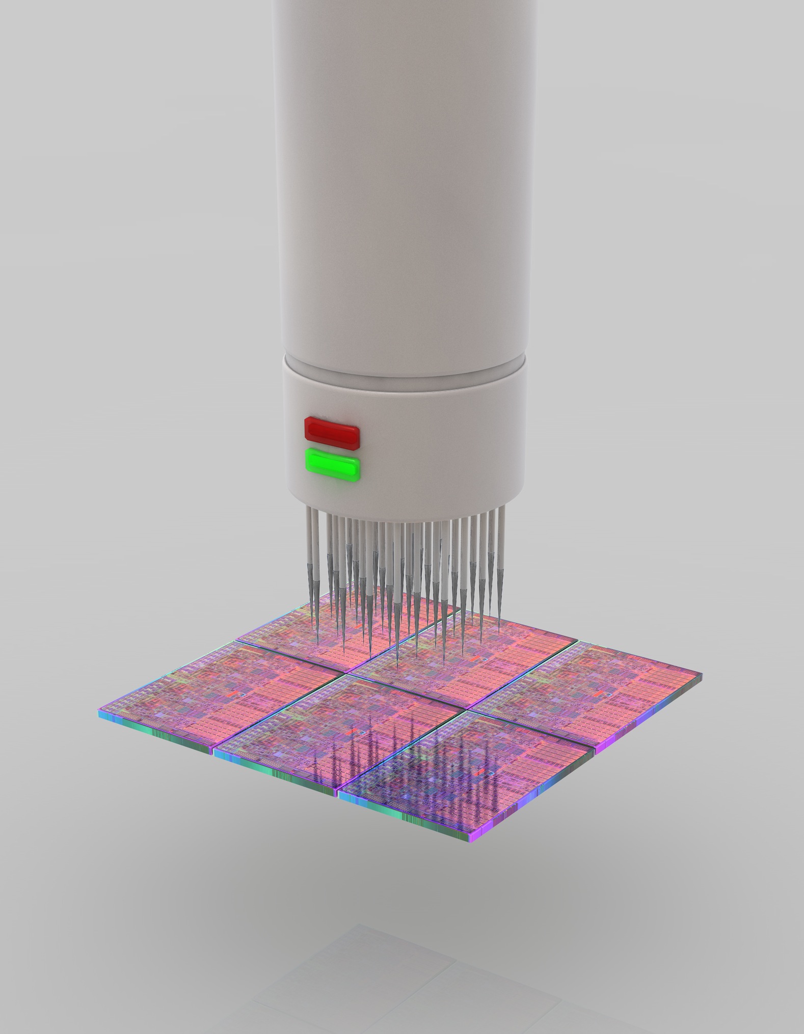
Intel Shows How A CPU Is Made
Intel released a press kit that visually explains how a CPU is made and reveals all the major steps in a process that normally takes hundreds of stages to complete. Check out the engineering magic!
Get Tom's Hardware's best news and in-depth reviews, straight to your inbox.
You are now subscribed
Your newsletter sign-up was successful
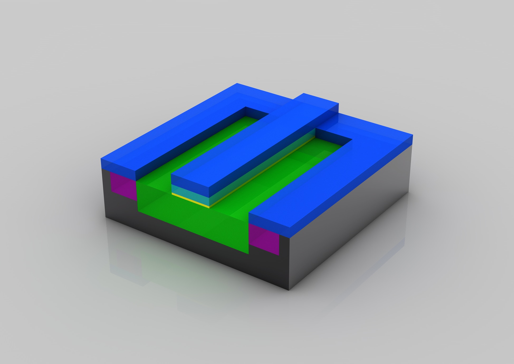
Reapplying More Photo Resist
More photo resist (blue) is applied and then re-exposed to UV light. Exposed photo resist is then washed off again before the next step, which is called ion doping. This is the step where ion particles are exposed to the wafer, allowing the silicon to change its chemical properties in a way that allows the CPU to control the flow of electricity.
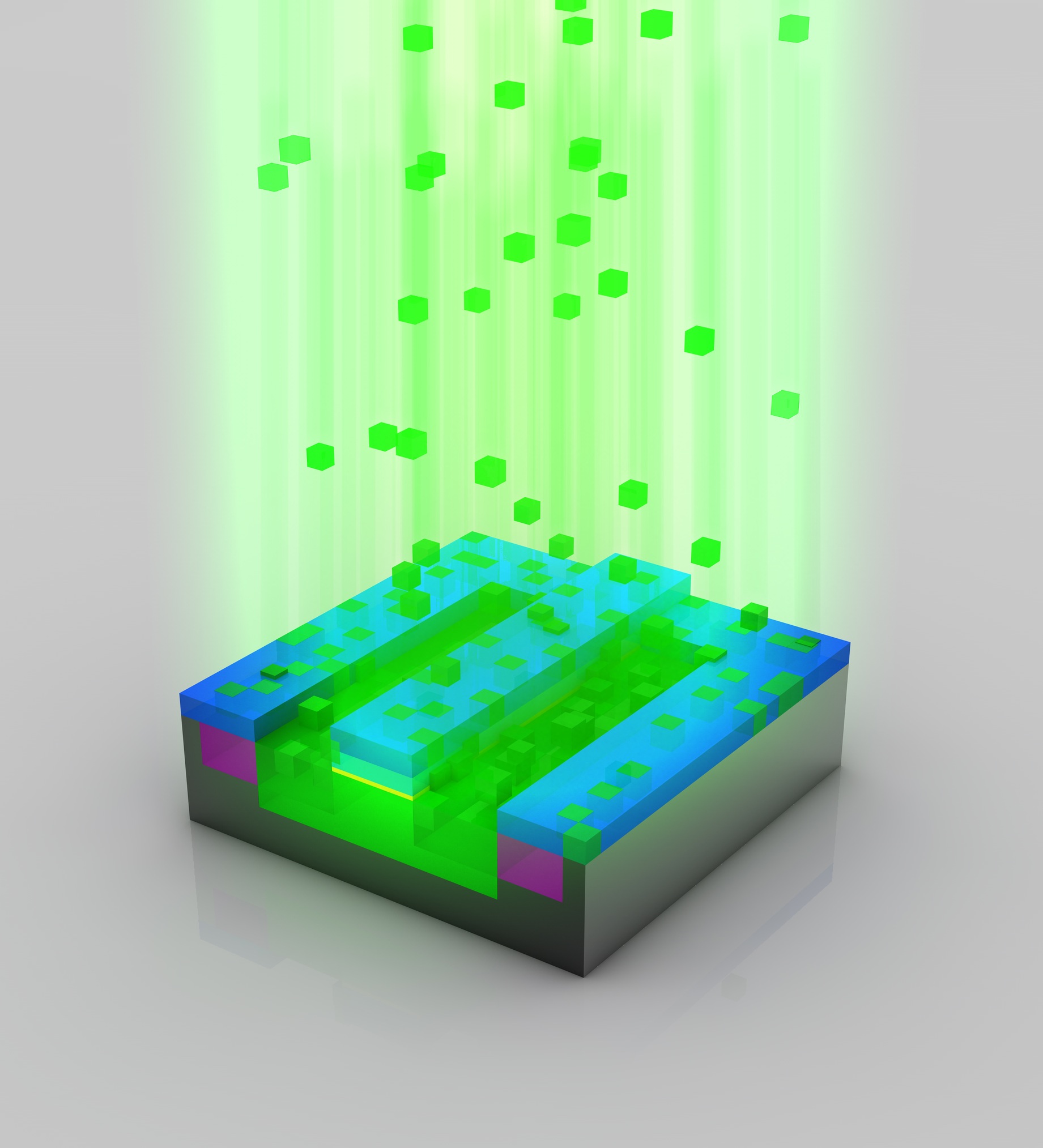
Ion Doping
Through a process called ion implantation (one form of a process called doping) the exposed areas of the silicon wafer are bombarded with ions. Ions are implanted in the silicon wafer to alter the way silicon in these areas conduct electricity. Ions are propelled onto the surface of the wafer at very high velocities. An electrical field accelerates the ions to a speed of over 300,000 km/hour (roughly 185,000 mph)
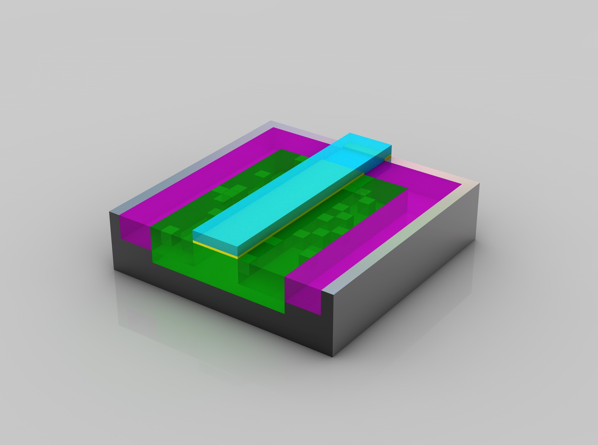
More Photo Resist Removal
After the ion implantation, the photo resist will be removed and the material that should have been doped (green) now has alien atoms implanted.
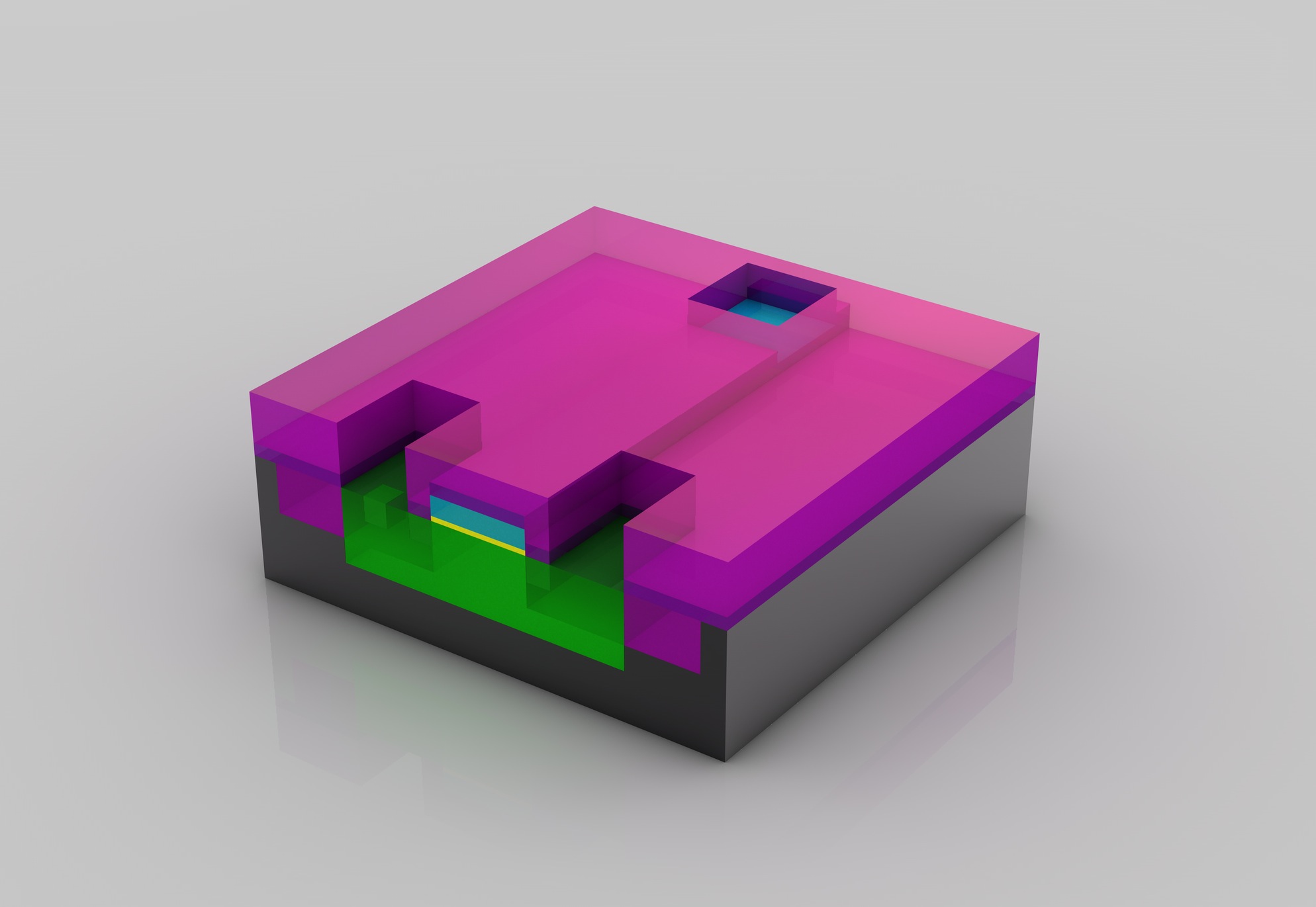
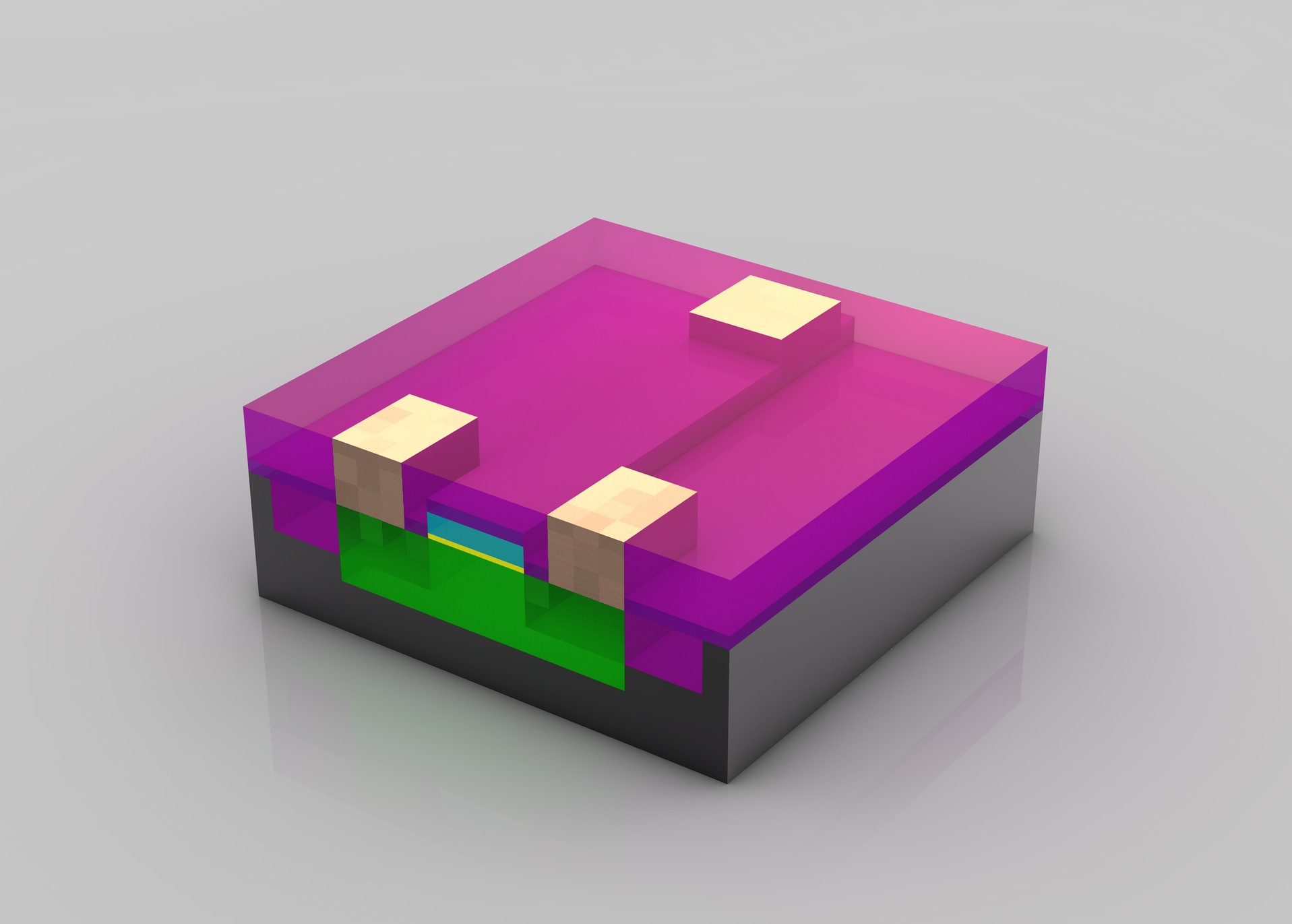
A Transistor
This transistor is close to being finished. Three holes have been etched into the insulation layer (magenta color) above the transistor. These three holes will be filled with copper, which will make up the connections to other transistors.
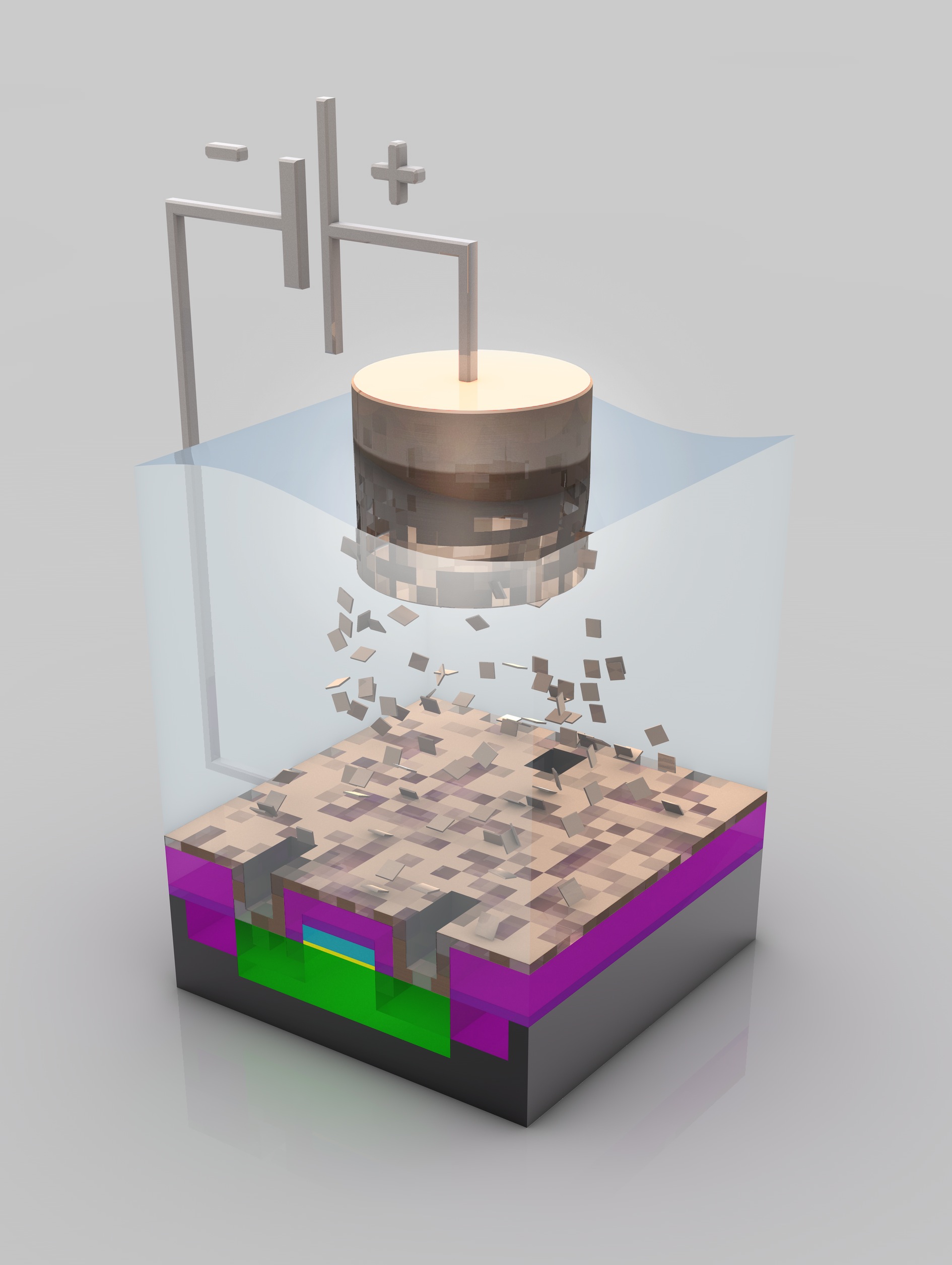
Electroplating The Wafer
The wafers are put into a copper sulphate solution at this stage. Copper ions are deposited onto the transistor through a process called electroplating. The copper ions travel from the positive terminal (anode) to the negative terminal (cathode) which is represented by the wafer.
Ion Settling
The copper ions settle as a thin layer on the wafer surface.
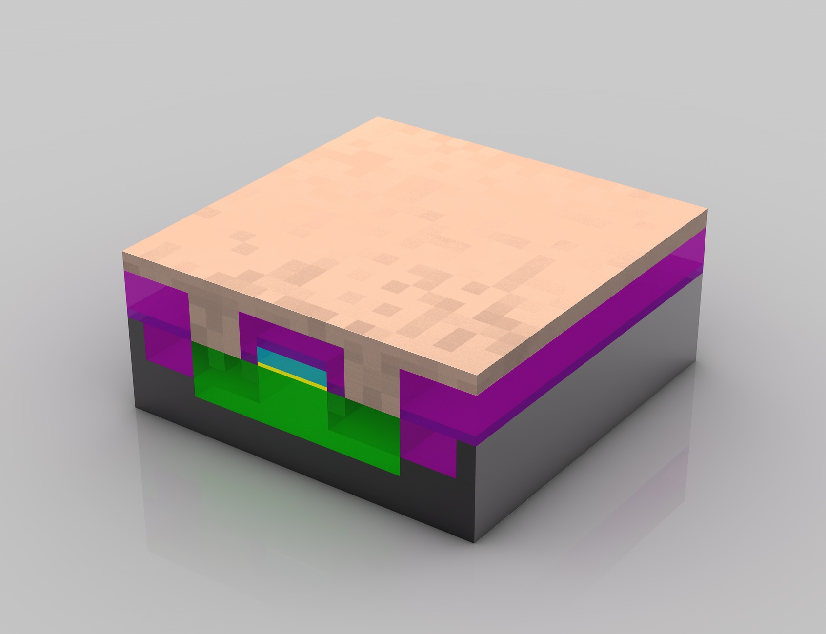
Polishing Excess Material
The excess material is polished off leaving a very thin layer of copper.
Get Tom's Hardware's best news and in-depth reviews, straight to your inbox.
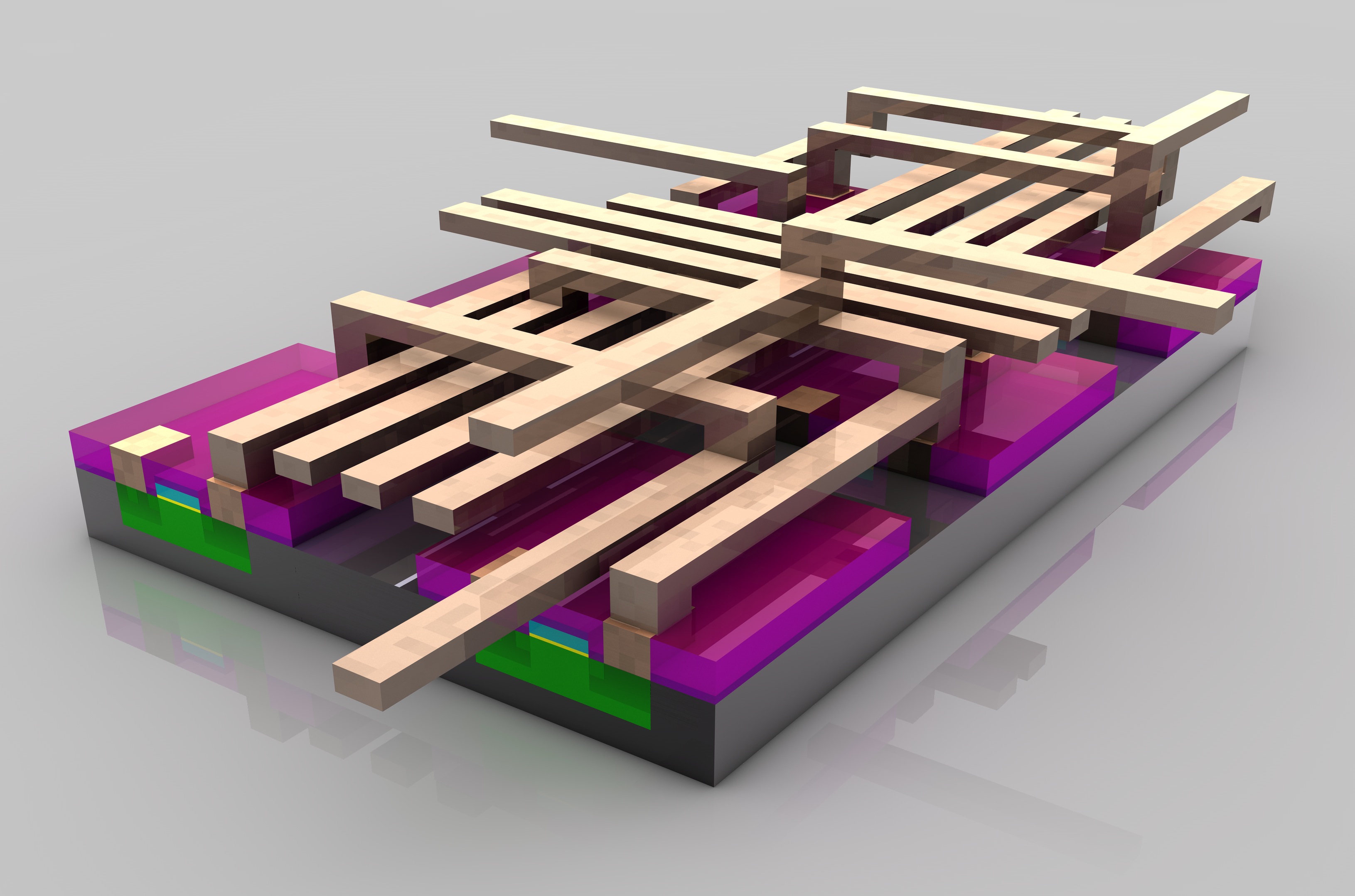
Layering
Multiple metal layers are created to interconnects (think wires) in between the various transistors. How these connections have to be “wired” is determined by the architecture and design teams that develop the functionality of the respective processor (for example, Intel’s Core i7 processor). While computer chips look extremely flat, they may actually have over 20 layers to form complex circuitry. If you look at a magnified view of a chip, you will see an intricate network of circuit lines and transistors that look like a futuristic, multi-layered highway system.
Wafer Sort Test
This fraction of a ready wafer is being put through a first functionality test. In this stage test patterns are fed into every single chip and the response from the chip monitored and compared to "the right answer."
Wafer Slicing
After tests determine that the wafer has a good yield of functioning processor units, the wafer is cut into pieces (called dies).
-
tacoslave http://cgi.ebay.com/Collectable-INTEL-Microchip-Keychain-w/-CPU-Steel-rope_W0QQitemZ360155521483QQcmdZViewItemReply
i want one of those keychains!! -
dmv915 tacoslavehttp://cgi.ebay.com/Collectable-IN dZViewItemi want one of those keychains!!Lol, this wouldn't happen to be your auction eh?Reply -
Bloodblender Saw this on APC's website, lol, pretty interesting stuff, but hey, at least Intel and AMD have got plenty of resources (sand) to keep making processors!Reply -
annihilator-x- Instead of 'sand' is the second most frequent chemical element, the article should say 'Silicon' is the second most abundant chemical element.Reply
Abundant is a better word as well as the fact that sand is mostly quartz among impurities and other minerals. Quartz itself is Silicon Dioxide crystals. -
nonamelab A little late Intel :) http://www.globalfoundries.com/multimedia/video/from_sand_to_chipReply -
rickzor I already know that a cpu can die due to overheat deteoration or due to electromigration, but that happens all during use. I always wondered how many years could a cpu or any other chip survive if always turned off!Reply
Maybe if turn off and praticly never used, our descendents could find perfectly working exemplars of our primitive cpus after what...2000 years or more!
Ah sorry about the relatively off topic subject, that's the efect of Life after people series on History Channel! -
Ryun nonamelabA little late Intel http://www.globalfoundries.com/mul nd_to_chipReply
Both of them were great. Thanks for the article, Toms, and thank you for the link.
