PrimeCables C05132 Charging Station Tear-Down: Organizational Power
Bottom
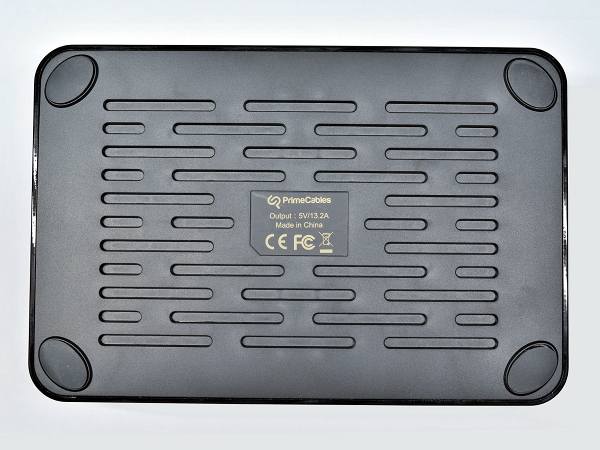
Aside from four feet, some recessed slots with no immediately obvious purpose, and the label, there isn’t a whole lot to see on the bottom cover. The label itself is unusually light on details, merely listing the brand, output rating, and country of origin, along with CE, FCC, and don’t-throw-in-trash logos.
I would have at least expected the model number on there, or even the input power specifications. Make the sticker hole bigger if you need to.
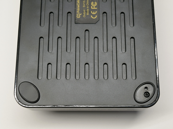
Rubber Feet Classic
When a product shows no obvious screws, and isn’t welded or glued together, there's a good chance that you'll find fasteners hidden under labels or rubber feet. Or both, as is the case here. Not only do these feet use fairly strong glue, but the holes themselves are so tight that they may hold the feet even without adhesive.
Article continues belowI thought I was home-free after removing five Phillips-head screws, but the cover remained firmly put.
Uncovered
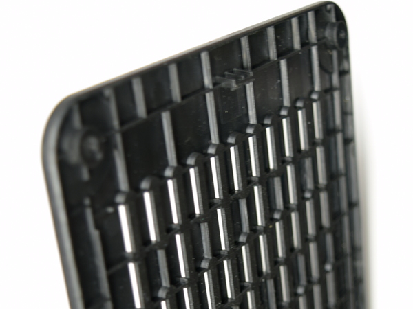
Many minutes of head-scratching and prying later, the cover finally came off. All of the slots that didn’t seem to do anything are actually ventilation slots opened sideways along most of their length. Since warm air rises and there are no openings on the top shell for it to escape through, I’ll allow myself to be skeptical about their effectiveness.
Near the top, about a centimeter from the cover’s edge, you’ll find a short plastic tab. That’s one half of the reason why this panel wouldn’t come off without a fight.
First Peek
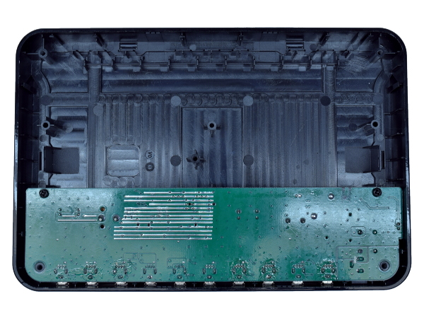
Above the screws holding the board at both ends, you’ll find two inaccessible plastic tabs sprouting from the shell. They were responsible for giving me such a hard time with disassembly. A lot of flex allowed them remain hooked as I tried prying and wiggling them apart.
Get Tom's Hardware's best news and in-depth reviews, straight to your inbox.
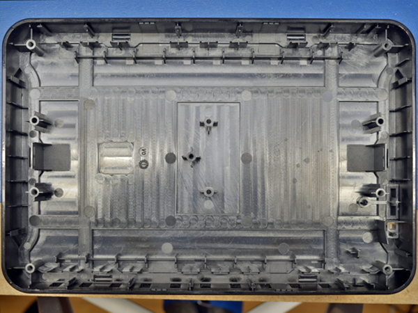
What’s inside the C05132’s significant desktop footprint? Mostly empty space with little more than an edge-to-edge ground plane across the board’s bottom. The body could have been a few centimeters narrower with little impact other than slightly less stability any time you drop a large tablet on top.
Shelled
Aside from the switch area in the bottom-right corner, everything else about the shell is symmetrical between the side with ports and the one without.
The only reason I can think of for including internal structures to support ports on both sides would be if its designer had visions of a variant with ports on both sides. Otherwise, simply rotate the internal mold 180° and you’re done.
Bottom Soldering
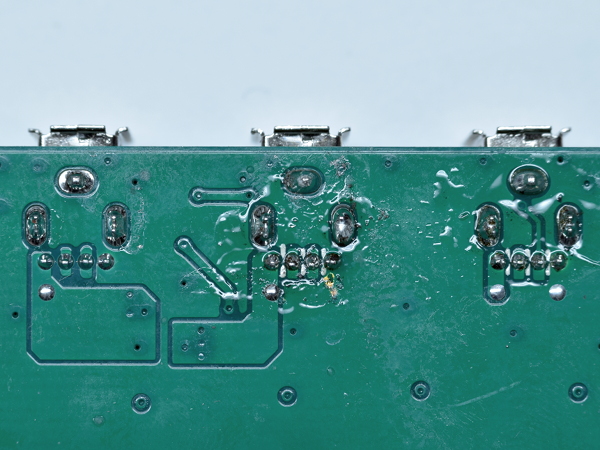
There isn’t a whole lot of soldering to look at aside from the USB ports and a handful of other through-hole components. What little there is ranges from fine-looking wave soldering on the left to OK-looking rework to the right and a botched patch job in the middle where some of the solder mask got scraped off.
Out of 10 ports, five received obvious rework. Was the solder wave set-up incorrectly? Did excess solder bath contamination cause inconsistent adherence? Inadequate flux distribution? Insufficient flux? Dirty or corroded connector pins? Whatever the case may be, results should be far better than this.
More Bottom Soldering
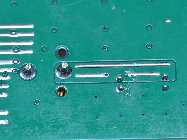
At first, I thought that some of the soldering hardships may have been caused by the large ground plane soaking too much heat. Then I noticed two picture-perfect solder joints for the output inductor’s leads (high thermal mass) next to perfectly fine soldering on the ground plane area with a pair of cruddy-looking joints in the middle of the fat trace. These small solder joints are for one of the two output polymer capacitors. For some reason, the middle joints are far worse than the second capacitor’s.
Whichever company manufactured this board, it needs to get its wave soldering quality control under control.
Station Board Top
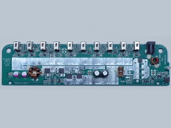
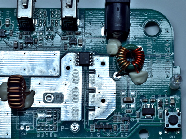
As far as circuit design goes, this looks straightforward enough: power comes in through the DC-in jack at the top-right, passes through a common-mode choke, the on/off switch circuitry in the bottom-right, an inductor for noise filtering, and a few capacitors at the DC-DC converter’s input. Then it passes through the DC-DC converter in the middle, some more capacitors at the DC-DC converter’s output in the bottom-left corner, and fans out to the ports over a wide and heavily tinned copper pour spanning most of the board’s top half.
The design is textbook-like, and the top-side soldering is also pretty good.
Input Area
In the DC input jack area, we find a common-mode choke that prevents common-mode noise from going either way across the connector, the on/off switch circuitry made entirely of discrete components powered by a 78L05 linear regulator, one populated 4435 (30V 20mΩ P-FET) out of four footprints gating power to the DC-DC converter, an unpopulated component cluster likely intended for fan speed control in the bottom-left corner, and the filter inductor.
During testing, this lone 4435 got lukewarm under full load, begging the question: why plan for four? My bet is on earlier production using far worse FETs.
DC-DC Converter Input Filter
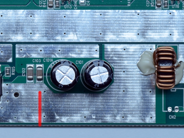
On the DC-DC converter input, a pair of large ceramic capacitors provides a low-impedance source to accommodate the converter’s high-frequency current peaks. A pair of 470µF 25V Jwco electrolytics handle bulk bypassing for the power cord, input inductor (likely doubling as an inrush current limiter), and on-off switch circuitry impedance.
As with any other high-frequency circuit, the ceramic bypass capacitors’ effectiveness could be improved by notching the copper pour in front of the MLCCs (red line) to focus the noise where they can affect it.
-
andrewpong Could you look at anker 5 port chargers, especially those with PowerIQ and QuickCharge features?Reply -
Daniel Sauvageau Reply
As far as I know at the moment, Power IQ appears to be Anker's trademark for using device identification chips, quite possibly the same CX1901/2901 and equivalents everyone else use.20905501 said:Could you look at anker 5 port chargers, especially those with PowerIQ and QuickCharge features?
As for QuickCharge, PassMark sent me one of its USB-PD testers and I was told they MIGHT implement QuickCharge support in the future. Right now, I'm waiting to hear more about how likely that is to happen while I decide how I am going to use the tester in the future, which currently means pestering PassMark with bug reports and feature requests to enhance its versatility.
I did receive three adapters with QC 3.0 support and a plain 5-ports adapter, two from Aukey, two from Anker courtesy from Roger. I could do tear-downs and test them as regular 5V adapters for now, then revisit them once I have something to emulate the protocol with. I could certainly start that batch from the 5-ports non-QC one and pit it against SilverStone's UC01.
At the moment, I have two more cube-style generic adapters in the publication pipeline and I'm partly done putting together a third one about a house-brand unit. (Spoiler: that third one is disappointing for unusual reasons. Though the 'unusual' could simply be because I am breaking into a new form-factor category - at least for me - on that one.) -
andrewmtl This is awesome for the party, if you host a party that is around 10 ppl, then you will love this little device, by the way, I believe that also had 2-3 faster charging port!Reply -
Daniel Sauvageau Reply
As I pointed out in the tear-down, two ports have dedicated 2.4A (2.6-2.65A measured) output each and a second pair is sharing a single 2.4A e-fuse, each pair using a CH2311 charger ID chip. The rest all do 1.4A with various resistor ID schemes.20938782 said:This is awesome for the party, if you host a party that is around 10 ppl, then you will love this little device, by the way, I believe that also had 2-3 faster charging port!
For offices, parties and mobile devices/gadgetry hoarders where function and convenience far outweigh efficiency, this sort of device can become a necessity.
