IDF 2000: Intel Pentium 4 (Willamette)
Get Tom's Hardware's best news and in-depth reviews, straight to your inbox.
You are now subscribed
Your newsletter sign-up was successful
Willamette Functionality
So what new features does the Willamette processor offer? Right from the start: the Willamette is still a 32 bit CPU and is intended to make its debut appearance at the end of the year with a clock speed of 1.4 GHz. Its similarity to the P6 core, which has been in existence since the Pentium Pro, is only rudimentary. Intel has incorporated interesting features in what will probably be the company's last 32 bit generation processor. Although the system bus is physically clocked at 100 MHz, the use of 'Quad Pump' technology increases the data transmission rate effectively to 3.2 GBytes/s. This is an increase of factor four in comparison with a Pentium III with a 133 MHz FSB and so it's as if the bus was clocked at 400 MHz. Similar tricks are known practice from DDR-II memories, AGP 4x and the Athlon EV6 bus; it simply means that more data is transmitted per clock cycle.
Intel declined to comment on the size of the L2 cache at this time. When I asked Albert Yu how much L2 cache memory the Willamette incorporated, he answered that he did not know. His brain had a 'memory problem'. An Intel employee later commented that he had known Albert Yu for several years and Albert had never had a 'memory problem'. :-)
The actual core of the Willamette has been subject to a general overhaul:
Article continues below- The Arithmetic Logical Unit (ALU) is clocked at twice the processor speed. Example: when the processor is clocked at 1.5 GHz, the ALU will be clocked at 3.0 GHz.
- Hyper Pipelined Technology. In comparison to a Pentium III the pipeline depth is now 20 levels instead of 10. At higher frequencies, this technology will be effectively scaled up.
- Intel has resized the floating point and multimedia engine to a 128 bit unit. Beyond this, the Streaming SIMD Extensions 2 have been introduced. The following table shows the changes clearly:
- MMXSIMDSIMD 2Integer64 Bit64 Bit128 BitFloating Point-Single (4x32 Bit)Double (2x64 Bit)
Tehama: Intel Rules The 400 MHz Bus With A Strict Hand
In a further attempt to extend its monopolistic position, Intel has pushed the chipset business. Didn't Andy Groves' keynote speech mention something about Intel's reorientation as an Internet and networking company?
And then the Tehama shocker arrives on the scene: Intel has accused the third party chipset manufacturer VIA Technologies of breach of contract. VIA allegedly activated the 133 MHz system bus in its Apollo Pro 133A chipset. Apparently, VIA should be satisfied with only 100 MHz although this would mean that the resulting products would yield lower performance. Whatever the case, Intel cancelled the license agreement. For VIA, future opportunities with the Willamette don't look too good. It is highly unlikely that VIA will ever get a license agreement for the Willamette. The second possible candidate ALI doesn't have any say in this scenario anyway.
Dirty Tricks: Rambus And The Stock Exchange
Intel's current roadmap, which was presented before the IDF, mentions an 'aggressive ramp-up' for Rambus memory (RDRAM). It's therefore not surprising that the one-and-only chipset Tehama supports this over-expensive memory type. That's the end of inexpensive SDRAM. Just before the IDF, the price of Rambus Inc. stock suddenly climbed. Intel outlined its future strategy for memory chips during the keynote: Rambus will be given preference over standard SDRAM. In a CNN interview, Intel confirmed once more that Tehama, the only chipset for the Willamette processor, will only support RDRAM. My personal impression of the reaction of certain 'analysts' in the press room was negative to say the least. That very same day they grabbed Rambus stock and recommended the same to their buddies. The stock rating of Rambus Inc. doubled within a short space of time - a real 'ramp-up'. To my mind, Intel was not fully aware of the consequences of this announcement, or were they? Let's not forget that the processor manufacturer has heavily invested in Rambus Inc.
The IA-64 Itanium For Servers/Workstations
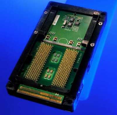
On the lower side of this Itanium CPU you can see the power connections, the lower half shows the pins for the socket connections and on top the PCB under which the L3 cache modules are located. The connection is named PAC418.
Get Tom's Hardware's best news and in-depth reviews, straight to your inbox.
Nothing for price-sensitive home users - that's the message. Intel's first 64 bit CPU 'Itanium' (previously code-named 'Merced') has been especially designed for servers and workstations and will be launched in late Fall in a 733 MHz version. Intel intends to follow it with an 800 MHz version at the end of the year. The Itanium is supported by the 460GX chipset, which can coordinate a maximum of four Itaniums simultaneously. Corresponding motherboards will utilize both sides of the board for a pair of CPU's (2x2) for this configuration. Maximum performance for these systems can only be expected where the operating system and applications have been ported to 64 bits. Intel has already invested in this area in order to ensure a successful introduction to the market. By the way, the 460GX works with DDR-SDRAM memories. That's right - SDRAM! When queried on this, the devious Albert Yu stated "we take account of our customers requirements". In other words: the use of Rambus memory would drive the cost of a server into the sky because servers or workstations are generally fitted with more memory than the 128 MB of an everyday consumer PC. Configurations using more than 1 GByte of RAM are not so uncommon. This decision is at least logical.

