Introducing Intel's 14nm Node and the Broadwell Processor
Intel finally provides solid information on Haswell's successor, the next-generation Broadwell core. We also learn some detailed info about the new 14nm processing node, a must-read for CPU enthusiasts who are interested in the future of Intel's Core!
Intel's 14nm Node and the Broadwell Core
The steps that Intel takes to update its processors are well documented, and old hat to anyone who follows the CPU industry. It is referred to as the company's "tick-tock" strategy, where the tick represents a node shrink that can squeeze more transistors into a smaller die, followed by a tock that indicates a significant architecture update. This repeats itself in a cycle of roughly a year and a half cadence. Last year's 22nm Haswell processor was a tock, so we're fast approaching the next tick: essentially a Haswell die shrink to 14nm, that tick is known as Broadwell.
If you're already familiar with this, then you already know what we expect from Intel's ticks: smaller processors, lower power usage, higher performance per watt, and similar overall performance compared to the previous generation product. That expectation shouldn't belittle the accomplishment as much as highlight the company's consistency over the last few product generations. What may surprise you is that this progression has resulted in a Haswell-Y processor with a TDP low enough to enable fanless enclosures less than 9 millimeters thick. That's an arena that Intel's Core brand has never ventured into before. But more on that later, let's start our analysis with the star of the show: Intel's new 14nm process node.
The 14nm Node: 2nd Generation FinFET
It might seem reasonable to assume that the numerical designation of a process node refers to a specific dimension (i.e. the 22nm node or 14nm node). While this was the case in early generations where the measurement corresponded to the smallest part of the transistor (usually the gate), this relationship no longer exists in modern nomenclature.
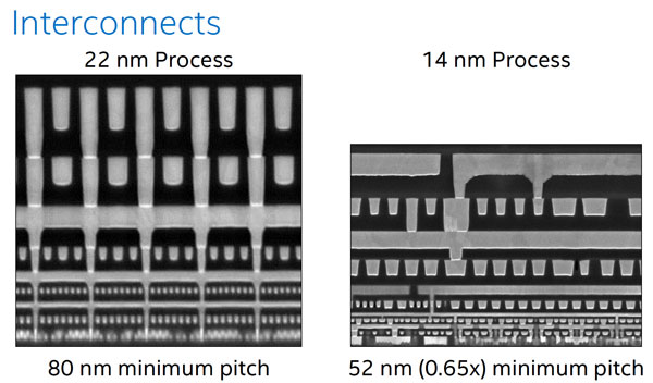
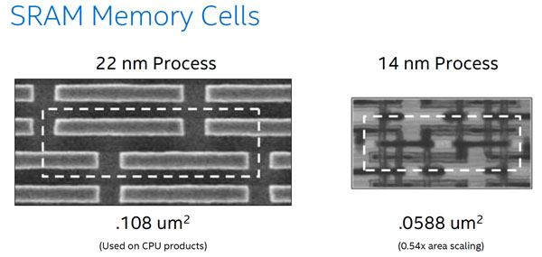
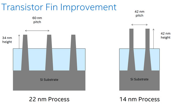
Article continues belowToday's nodes are named after a theoretical representation designed to indicate its average physical scale relative to previous generation nodes. For example, if we compare Intel's 22nm to 14nm nodes, we find that transistor fin pitch (the space between fins) has been reduced from 60nm to 42nm, transistor gate pitch (the space between the edge of adjacent gates) has gone from 90nm to 70nm, and the interconnect pitch (the minimum space between interconnecting layers) has changed from 80nm to 52nm. An SRAM memory cell that takes up 108 square nanometers of area on the 22nm node scales down to 59nm2 on the 14nm node.
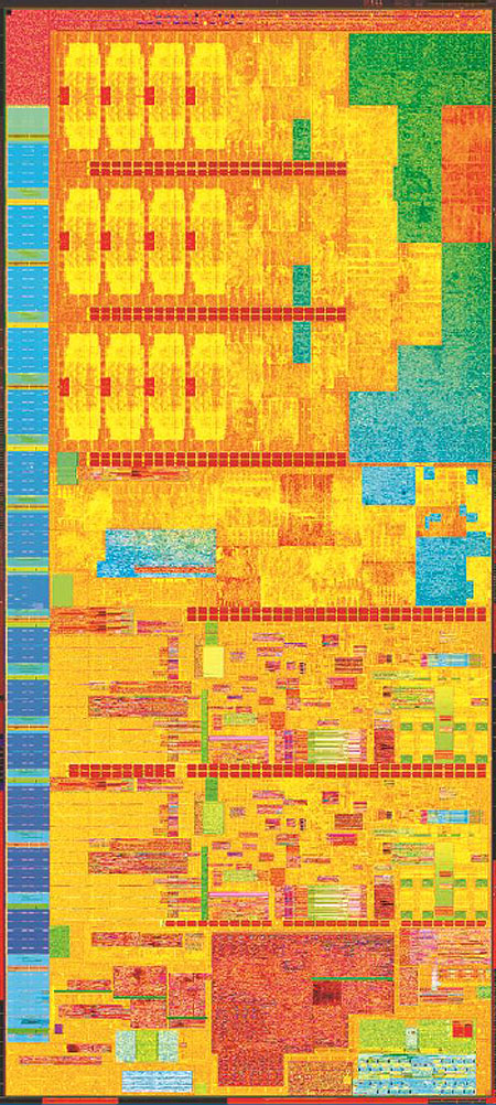
Those dimensions range from a scaling factor of 0.70x (the transistor fin pitch size) to 0.54x (SRAM memory cell area scaling). If you take the number 22 and multiply it by 0.64x you end up with about 14, so it's probably fair to say that Intel assigned an appropriate numerical designation to its 14nm process node. In fact, the Broadwell-Y die has about 63% less area than the Haswell-Y die.
Intel's 22nm node is the company's first-generation FinFET (also known as Tri-Gate) transistor design. The new 14nm process represents Intel's second-generation FinFET, with a tighter fin pitch for improved density. Combining this with taller and thinner fins results in higher drive current and better transistor performance. The number of fins per transistor has been reduced from three to two, which also improves density while lowering capacitance.
Intel's competitors are currently transitioning from MOSFET to FinFET transistor designs, but the company claims that it has a competitive edge when it comes to logic area scaling. Based on published information from TSMC and the IBM alliance, and using the scaling formula (gate pitch x metal pitch), Intel claims that TSMC's upcoming 16nm node yields no logic area scaling improvement over 20nm and that the competition will trail significantly for the next two generations. Of course this formula is only one metric, but it does make us curious to see how TSMC's 16nm node will perform once it is implemented next year. We also have to wonder if the laws of physics won't become an insurmountable barrier under 10nm, which may give the competition some time to catch up to Intel. Having said that, Moore's Law appears to continue unabated for the moment.
Get Tom's Hardware's best news and in-depth reviews, straight to your inbox.
Let's quickly touch on yields. No semiconductor company is completely transparent when it comes to this topic, but Intel did share a few tidbits of information. In general terms, Intel told us that its 22nm process produces the highest yield of the past few node generations, and that the 14nm Broadwell SoC yield is in a healthy range and trending in an optimistic direction. The first products are qualified and currently in volume production, with expected availability at the end of 2014.
The point of all this is that leakage, power usage, and the cost per transistor is reduced, while both performance and performance per watt is increased compared to the previous-generation node. As we said, none of this is a surprise but it's always a welcome change, especially if it enables new usage models. That comes into play when we consider the actual products that Intel will ship on the 14nm node. One of those products is Broadwell-Y, the next-generation mobile chip that Intel shared the most details on. We'll talk more about that on the next page, but let's consider the general architectural improvements that will be leveraged across all Broadwell-based processors first.
The Broadwell Converged Core
Intel claims that Broadwell boasts at least a 5% IPC increase over Haswell. That's a minor difference, but not much of a surprise considering that this is a process improvement tick and not a new architecture tock.
As such, the improvements are mostly the result of beefing up existing resources, not re-engineering them. The 14nm node density improvement was successful enough to allow Intel more room to add transistors, so they did: a larger out-of-order scheduler (Intel didn't specify the size difference) results in faster store-to-load forwarding. The L2 Translation Lookaside Buffer (TLB) has been increased from 1k to 1.5k entries, and a new 1GB/16 entry page of L2 was added. A second TLB page miss handler was added so that page walks can now be performed in parallel.
The floating point multiplier is much more efficient, now able to accomplish in three clock cycles what takes Haswell five cycles to complete. Broadwell also has a radix-1,024 divider and is purportedly faster at performing vector gather operations. Intel also asserts that branch predictions and returns are improved.
Aside from these general areas, some specific functionality was targeted. Cryptography acceleration instructions are improved, and virtualization round-trips are faster. Of course, power usage reduction is high on Intel's priority list, and the company claims that it only spent transistors on the features that add performance with a minimal power cost. On the next page, we'll learn more about some of the power gating and efficiency optimizations that Intel implemented in Broadwell.
- 1
- 2
Current page: Intel's 14nm Node and the Broadwell Core
Next Page Broadwell-Y: The Intel Core M ProcessorDon Woligroski was a former senior hardware editor for Tom's Hardware. He has covered a wide range of PC hardware topics, including CPUs, GPUs, system building, and emerging technologies.
-
Mike Stewart Nope... still not good enough !Reply
at 4.6Ghz my 2700K is more than a capable CPU .
Bring on the Skylake,, then we'll talk . -
InvalidError With Intel heavily focusing on power-efficiency, my bet is clocks are not going to get bumped by more than 200MHz, quite possibly less: by collapsing the multiplier pipeline from five cycles to three and supersizing a bunch of other things, that is a whole lot more logic per stage and of those additions chip away at any timing closure margins that may have been gained from the shrink.Reply
I would expect this to also translate into even more unpredictable and voltage/temperature-sensitive overclock outcomes. -
Shneiky 2700K at 4.0/4.4 turbo 1 core for silent operation. Guess this year, I will change the Evo to something beefier and go 4.2 or 4.3 with 4.6 as a turbo to remain silent. Rocking 2011 year gear and still not finding a reason to upgrade. For a person who renders almost all the time, this CPU stagnation is frustrating.Reply -
Gaurav Rai Its good to see Intel working so hard on their thermal department. Gaming is great, but you cant help feeling guilty about mother earth every time you fire up your pc. Meanwhile Amd innovates with 220W processor XDReply -
ceeblueyonder intel need die shrinks to cram in their specializalize units or cpu's. i am not really sure. but, intel has a bunch of specialize instructions built into their chips to beef it up, make it have faster ipc but also relying on software to take advantage of it. things like quicksync comes to mind or the SSE or whatever it is called. in comparison, amnd chips like the fx-series chips and the phenoms before it seems simpler, to me. a more general computing unit. kind of like powerpc chips or arm chips. they compose of execution cores or integer cores and floating point units and thats it. no instruction sets and quicksync decoders to gain software-driven advantage. but i don't really know. just hunches. i tend to make hunches but hopefully, they're educated hunches. so i am rooting for amd! intel's die shrinks seems to be like a monopolistic grip that keeps others with better "Architectures," simpler more general logical integer units to stay behind. since these cores with die shrinks, say an amd at 14nm, too would probably blow the top off of a competing intel that is also at 14nm. again, general computing units which i think AMD, IMB POWERPC, ARM chips have an inherent advantage to intel's inferior x86 architecture. AMD and POWERC both were the first x64 cpu's. but i could be wrong. again, just a hunch. intel blows amd out of the water today b/c intel has chips at 14nm, competing with AMD that has 32nm or 28nm chips. and also the software-driven instruction sets that intel has crammed into their chips that make software developers basically just check a box or intel has supported them to make intel chips run even faster than say AMD, which doesn't have quicksync or SSE or whatever it's called.Reply
thus beat amd. but, to me, amd chips like the fx-series and the phenoms before have a simplicity to them that i admire. although i can't specifically say how or what it is. -
qlum While better efficiency is nice and all I fear intel won't do enough for gamers to warrant an upgrade of their cpu. When overclocked Haswell doesn't do much above Sandy bridge and while intel may not have the strongest competition from amd on the higher end anymore if people won't upgrade their cpu's it will hurt them on the longer run.Reply
-
InvalidError Reply
Can you really call it innovation when AMD needs a 200W chip to compete with Intel's sub-100W chips? Unless you meant innovation in the high-tech space-heater market.13933630 said:Meanwhile Amd innovates with 220W processsor XD
Intel has gone down the crank-clocks-power-be-damned path with Prescott about a decade ago and that did not work too well. AMD just tried the same thing and "shockingly," that did not work particularly well for them either. -
ceeblueyonder it's also odd that intel is the die shrink boy. die shrink cpu company doing all the die shrinks. perhaps, the die shrink industry can only support one coompany at a time. as if, supporting two companies that are also doing tick tocks would "saturate" the indsutry too much. it probably has a lot to do with greed. money. but, that doesn't matter. what we all need to know is that just because intel beats amd today doesn't mean intel makes better chips. or that intel has superior technology. we need to take a closer look at what intel is doing and what amd is not doing and then look at their products more closely than just geekbench scores or ceinbench scores. look under the hood.Reply -
Shneiky @InvalidError,Reply
What Gaurav Rai said:
"Meanwhile Amd innovates with 220W processsor XD"
Was humor. You know, like Ha-ha and stuff? -
InvalidError Reply
Even if you compare Sandy Bridge (32nm) Intel CPUs with AMD's FX83xx (28nm) which theoretically gives the advantage to AMD, Intel's older chips still win most benchmarks. Intel being one process node ahead has very little to do with their performance lead; their architecture itself is just that far ahead.13933740 said:intel blows amd out of the water today b/c intel has chips at 14nm, competing with AMD that has 32nm or 28nm chips.


