Introducing Intel's 14nm Node and the Broadwell Processor
Intel finally provides solid information on Haswell's successor, the next-generation Broadwell core. We also learn some detailed info about the new 14nm processing node, a must-read for CPU enthusiasts who are interested in the future of Intel's Core!
Broadwell-Y: The Intel Core M Processor
Broadwell-Y: Introducing the Intel Core M Processor
The new 14nm node will be leveraged across multiple product segments, from data centers to tablets,via three separate Broadwell dies. For now Intel limited the information it shared with us to the mobile-oriented Broadwell-Y chip. We are told to expect an increasing amount of details on the other Broadwell products over the next quarter, with more to come during next month's Intel Developer Conference (IDF), but for now we'll have to remain content with details about the low-power mobile spin of this chip. Of course, improvements to the Broadwell core architecture will be reflected in the other dies, too. With that in mind, let's take a closer look at Broadwell-Y, marketed under the Intel Core M moniker.
The new Core M brand will cover all of the mobile space, and Intel told us that other brands like the Celeron and Pentium M will not be applied to the Broadwell-Y SoC. While the company did not disclose any actual model numbers or clock speeds, it stressed the new chip's capability to drive a hypothetical 7 to 10mm-thick fanless form factor with a 10.1" display, enabled by a 3 to 5W version of this processor. We were allowed to handle a working prototype in the form of a sexy 7mm-thin tablet, but were not allowed to run any software or examine specifications via the control panel. Until we have a working model to test, we'll have to take Intel's word that Broadwell-Y provides a "greater than 2x reduction in TDP with better performance than Haswell-Y".
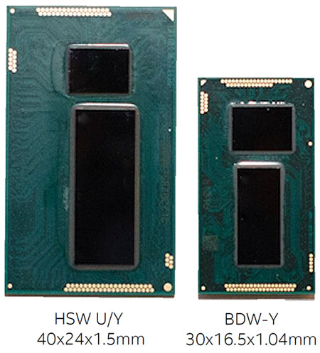
We do have some specifics when it comes to the die and package sizes though. The Broadwell-Y chip is 82mm2, scaled down about 63% compared to Haswell-Y's 130mm2 die size. As for the board package, Broadwell-Y has a 50% smaller surface area and 30% thinner package compared to Haswell-Y. Part of this reduction is made possible by the relocation of the 3DL modules to a separate, tiny PCB that is attached to the bottom of the Broadwell-Y package. Of course, motherboards will need to have an appropriately-sized hole cut to accommodate it.
Article continues belowBecause area scaling was better than expected on the 14nm node, Intel added 20% more transistors for increased features and performance. For instance, Haswell-Y's integrated graphics has a maximum of 20 AUs, while Broadwell-Y can use up to 24. That's 20% more compute resources, and Intel also claims a 50% increase in graphics sampler throughput. The company also mentions geometry, Z, and pixel fill performance improvements due to micro-architecture changes, though the company hasn't yet been specific about what these are. 4K display compatibility was also trumpeted, and two of them are theoretically supported, but practical power draw limits for a mobile device probably make this an unlikely scenario.
Intel's Core M: Focused on Low Power
Intel claims that the Broadwell-Y 14nm design and process optimizations account for the 2x lower power than Haswell-Y, which enables fanless functionality. The key SoC statistics include 25% lower power thanks to capacitance improvements, 20% less power thanks to lower minimum voltages combined with design optimizations, up to 15% improved transistor performance at low voltages, about a 10% reduction in power thanks to lower transistor leakage, and a smaller, denser processor. Of course, Intel hasn't disclosed the specific TDPs of the products that they've based these claims on, so we'll have to wait a bit longer for more information. We do know that the chips Intel is talking about have a 10 to 15W high burst speed for quick response, followed by a three to four watt sustained operating speed a few milliseconds later under load.
Broadwell-Y features the second-generation implementation of Intel's Full Integrated Voltage Regulator (FIVR), which can speed the transition between idle and load clock states. FIVR now features non-linear droop control, and a new dual FIVR LVR mode has been added. It turns out that FIVR is not particularly efficient at very low voltages, so it can now be bypassed when necessary to save power.
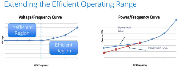
The SoC has an extensive list of optimizations that target active power reduction: design process optimization to reduce minimum operating voltage and dynamic capacitance (Cdyn), a re-architecture of DDR/IO/PLL/Graphics, optimizations for Cdyn in IA/Graphics/PH, and lower operating frequency ranges for IA/GT and Cache. There are other enhancements, too, such as dynamic display voltage resolution. Graphics can be controlled by Duty Cycling Control (DCC) to reduce usable power, or even turn it on and off as necessary. The latency needed to switch the GPU on and off is negligible, and it can be reduced to as low as 12.5% of its rated operating frequency.
Get Tom's Hardware's best news and in-depth reviews, straight to your inbox.
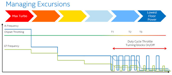
Clock rates are, of course, tied to both power usage and thermal output. Three boost states are leveraged to deliver the highest possible clocks while maintaining system stability. The PL3 boost state allows the most amount of power that won't damage the system's battery, used for very short spikes as needed - the kind of time spans that are measured in milliseconds. PL2 is the standard burst limit, and PL1 represents the long-term system limit of sustainable power delivery. If necessary, duty cycle throttling can turn blocks of the processor on or off to minimize power usage and heat generation.
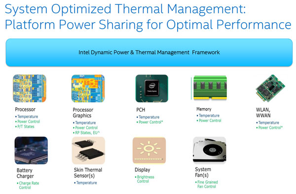
The power and thermal management framework is handled on a system level, by tracking multiple components to measure and change as necessary. This is controlled via Intel's Dynamic Power and Thermal Management software driver.
Intel's Platform Controller Hub (PCH) has also been re-engineered for Broadwell with an eye toward power efficiency. Idle power has been reduced by 25% compared to 2013, and active power has been dropped by 20% versus Haswell's PCH-LP. There are new power domains, and a new power reduction in firmware, hardware, and software updates which include fine-grain monitoring and reporting.
In addition to power enhancements, the PCH has been improved with an Audio DSP upgrade that includes more SRAM and higher MIPS. Advanced post-processing is available, with new wake-on-voice functionality. There are also fresh management and security features. Note that the PCH is manufactured using the 22nm node, so it hasn't shrunk.
Conclusion: Promising Statistics For Intel's Core M
We probably won't have access to test Intel's Broadwell CPU for a few months at least, but based on what we've seen, the company has lived up to the lofty expectations it has set. As we mentioned in our introduction: smaller processors, lower power usage, higher performance per watt, and similar overall performance compared to the previous generation at comparable clocks. All of those attributes are very desirable from a consumer standpoint.
But a lot of questions remain this early in the game. What kind of clock rates can we expect from Intel's 14nm node? How will the GPU scale compared to Haswell? What kind of Core M pricing can we expect, and will it be low enough to inject some life into low-cost Intel tablets? All of these questions will be answered over time, and we hope that at least some of them will be answered at IDF next month. Until then, we can certainly see a lot of potential in the upcoming Broadwell line.
- 1
- 2
Current page: Broadwell-Y: The Intel Core M Processor
Prev Page Intel's 14nm Node and the Broadwell CoreDon Woligroski was a former senior hardware editor for Tom's Hardware. He has covered a wide range of PC hardware topics, including CPUs, GPUs, system building, and emerging technologies.
-
Mike Stewart Nope... still not good enough !Reply
at 4.6Ghz my 2700K is more than a capable CPU .
Bring on the Skylake,, then we'll talk . -
InvalidError With Intel heavily focusing on power-efficiency, my bet is clocks are not going to get bumped by more than 200MHz, quite possibly less: by collapsing the multiplier pipeline from five cycles to three and supersizing a bunch of other things, that is a whole lot more logic per stage and of those additions chip away at any timing closure margins that may have been gained from the shrink.Reply
I would expect this to also translate into even more unpredictable and voltage/temperature-sensitive overclock outcomes. -
Shneiky 2700K at 4.0/4.4 turbo 1 core for silent operation. Guess this year, I will change the Evo to something beefier and go 4.2 or 4.3 with 4.6 as a turbo to remain silent. Rocking 2011 year gear and still not finding a reason to upgrade. For a person who renders almost all the time, this CPU stagnation is frustrating.Reply -
Gaurav Rai Its good to see Intel working so hard on their thermal department. Gaming is great, but you cant help feeling guilty about mother earth every time you fire up your pc. Meanwhile Amd innovates with 220W processor XDReply -
ceeblueyonder intel need die shrinks to cram in their specializalize units or cpu's. i am not really sure. but, intel has a bunch of specialize instructions built into their chips to beef it up, make it have faster ipc but also relying on software to take advantage of it. things like quicksync comes to mind or the SSE or whatever it is called. in comparison, amnd chips like the fx-series chips and the phenoms before it seems simpler, to me. a more general computing unit. kind of like powerpc chips or arm chips. they compose of execution cores or integer cores and floating point units and thats it. no instruction sets and quicksync decoders to gain software-driven advantage. but i don't really know. just hunches. i tend to make hunches but hopefully, they're educated hunches. so i am rooting for amd! intel's die shrinks seems to be like a monopolistic grip that keeps others with better "Architectures," simpler more general logical integer units to stay behind. since these cores with die shrinks, say an amd at 14nm, too would probably blow the top off of a competing intel that is also at 14nm. again, general computing units which i think AMD, IMB POWERPC, ARM chips have an inherent advantage to intel's inferior x86 architecture. AMD and POWERC both were the first x64 cpu's. but i could be wrong. again, just a hunch. intel blows amd out of the water today b/c intel has chips at 14nm, competing with AMD that has 32nm or 28nm chips. and also the software-driven instruction sets that intel has crammed into their chips that make software developers basically just check a box or intel has supported them to make intel chips run even faster than say AMD, which doesn't have quicksync or SSE or whatever it's called.Reply
thus beat amd. but, to me, amd chips like the fx-series and the phenoms before have a simplicity to them that i admire. although i can't specifically say how or what it is. -
qlum While better efficiency is nice and all I fear intel won't do enough for gamers to warrant an upgrade of their cpu. When overclocked Haswell doesn't do much above Sandy bridge and while intel may not have the strongest competition from amd on the higher end anymore if people won't upgrade their cpu's it will hurt them on the longer run.Reply
-
InvalidError Reply
Can you really call it innovation when AMD needs a 200W chip to compete with Intel's sub-100W chips? Unless you meant innovation in the high-tech space-heater market.13933630 said:Meanwhile Amd innovates with 220W processsor XD
Intel has gone down the crank-clocks-power-be-damned path with Prescott about a decade ago and that did not work too well. AMD just tried the same thing and "shockingly," that did not work particularly well for them either. -
ceeblueyonder it's also odd that intel is the die shrink boy. die shrink cpu company doing all the die shrinks. perhaps, the die shrink industry can only support one coompany at a time. as if, supporting two companies that are also doing tick tocks would "saturate" the indsutry too much. it probably has a lot to do with greed. money. but, that doesn't matter. what we all need to know is that just because intel beats amd today doesn't mean intel makes better chips. or that intel has superior technology. we need to take a closer look at what intel is doing and what amd is not doing and then look at their products more closely than just geekbench scores or ceinbench scores. look under the hood.Reply -
Shneiky @InvalidError,Reply
What Gaurav Rai said:
"Meanwhile Amd innovates with 220W processsor XD"
Was humor. You know, like Ha-ha and stuff? -
InvalidError Reply
Even if you compare Sandy Bridge (32nm) Intel CPUs with AMD's FX83xx (28nm) which theoretically gives the advantage to AMD, Intel's older chips still win most benchmarks. Intel being one process node ahead has very little to do with their performance lead; their architecture itself is just that far ahead.13933740 said:intel blows amd out of the water today b/c intel has chips at 14nm, competing with AMD that has 32nm or 28nm chips.


