Intel-Micron 3D XPoint At Xroads
Today we're sorting out what's happened with Intel and Micron's 3D XPoint collaboration since it was announced in late July.
Get Tom's Hardware's best news and in-depth reviews, straight to your inbox.
You are now subscribed
Your newsletter sign-up was successful
What We Still Don’t Know
How It Actually Works
Which is to say, what is the bulk property change technology in play?
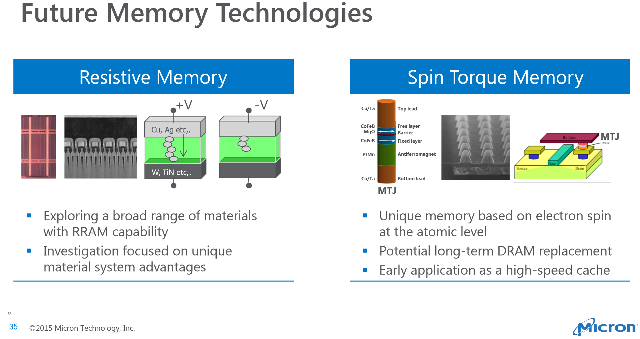
In a sit-down chat with Crooke during IDF, we asked him three different ways what technology 3D XPoint was using. His first answer was simply that it was new and it is 3D XPoint. He also wondered why everyone was so focused on the property change mechanism (some have said PCM, some ReRAM), saying, "it’s recreational to some extent how we’re accomplishing that." His third reply was simply that it was a competitive advantage, meaning we won’t know until it is impossible for Intel to keep it from us.
Given that Intel’s SSD market share is a fraction of Samsung’s, even with Micron’s share thrown on top, we suppose it’s understandable. Intel isn't accustomed to playing second fiddle. According to TrendFocus, Intel continues to dominate the enterprise PCIe market, but Samsung has a monstrous lead in total exabyte output and units sold.
Article continues belowEven details from Micron's latest Analyst Conference do little to clarify the type of memory employed in 3D XPoint. At any given time, the company has up to 26 different memory technologies under evaluation.
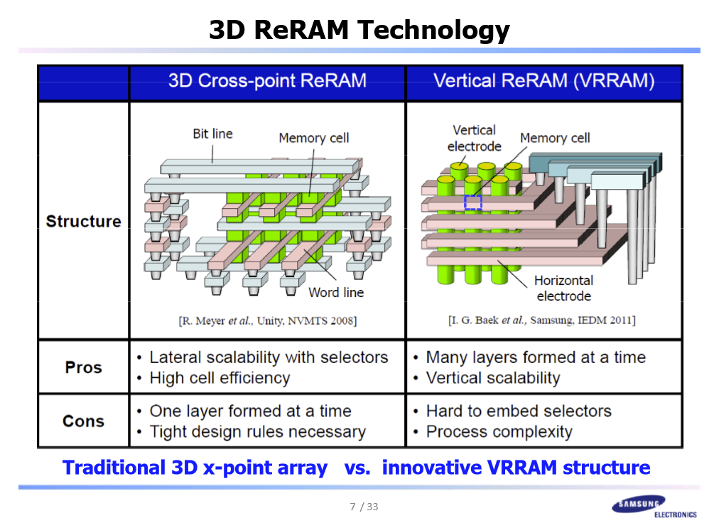
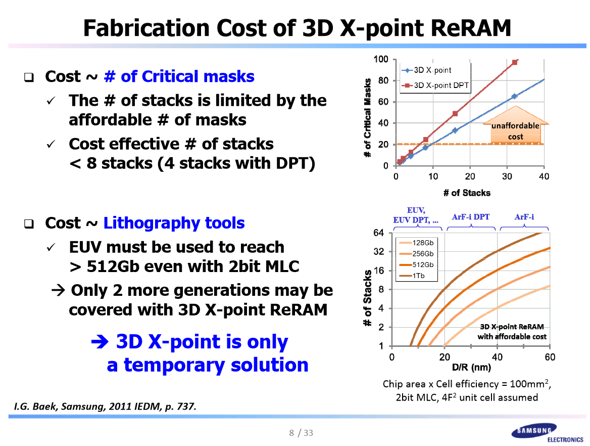
Speaking of Samsung, a presentation from 2012 referenced the idea of using what the company termed a “3D Cross-point ReRAM” architecture, and called into question its long-term scalability. Samsung was suggesting at the time that a Vertical ReRAM (VRRAM) architecture would be more effective and scalable in the long term, whereas ReRAM-based "3D x-point" would only be a temporary solution.
In other words, this architecture is not new, and in fact Samsung rejected it because the company didn't think it had longevity, at least according to that presentation. However, Crooke thinks it does, and addressed 3D XPoint scalability by pointing out that the lithography issues are pretty simple to solve with this architecture, and that Intel can add more layers, but can also bring the pillars closer together.
DIMMs And JEDEC Compliance
One new item Crooke revealed on stage at IDF was that 3D XPoint would ship in memory-mapped devices (DIMMs). We asked him whether they'd be JEDEC-compliant and he replied they'd be compatible with DDR4 mechanically and electrically, but that the technology would require a new interface since it is non-volatile, and that Intel was integrating it into its platforms.
Get Tom's Hardware's best news and in-depth reviews, straight to your inbox.
An audience member asked Geof Findley, Intel's memory ecosystem director, "Is the protocol for 3D XPoint going to be identical to DDR4 DRAM?" Findley answered evasively: "It will plug into a DDR4 socket. Next question."
When asked if it was an NVDIMM by JEDEC standards, Findley answered, simply, "No." When asked if it will leverage a proprietary protocol that would remain proprietary to Intel, he answered, simply, "Yes." Moreover, when asked again whether it would be JEDEC-compliant, he replied, "Not at this time."
There are your answers, delivered with dental forceps.
It appears the specter of a proprietary interface looms menacingly on the horizon, which is fomenting a dire sense of foreboding in the industry. During a recent standing room-only presentation at the Flash Memory Summit, the mere mention of the requirement for a proprietary interface cast a pall over the audience. Such an outcome could hamper adoption and put quite a bit of unbridled power in the hands of Intel and Micron. Intel already has a great deal of control at the CPU and chipset level due to a lack of competitors.
Findley clarified that the 3D XPoint support would only be applicable to a future Xeon processor. He specifically stated that support was not due on the Grantley refresh, but rather the following generation.
Will performance and cost be closer to DRAM or NAND?
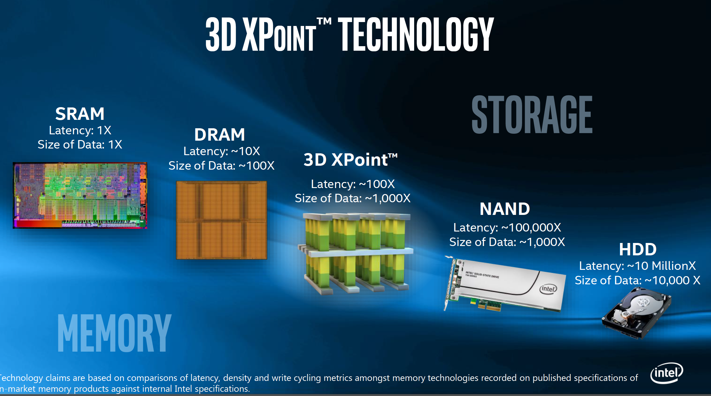
Intel tossed around some high-level figures, but was not specific. There was no discussion about pricing, even on a percentage basis.
SRAM is the baseline in the chart above. As you can see, among other things, the capacity points will be the same as NAND, but offer a 1000x performance increase when measured solely in latency.
Intel has been a staunch proponent of the new NVMe (Non-Volatile Memory Express) protocol, a lightweight register interface constructed from the ground up with future non-volatile memory technologies in mind (not NAND).
In fact, Intel established the NVMe standards committee, which consists of every major memory manufacturer. Intel recently revealed that it founded the NVMe development committee specifically with the goal to provide a refined interface to empower 3D XPoint-based products. Yes: In an odd twist of fate, Intel’s own competitors helped pour fuel onto the 3D XPoint fire.
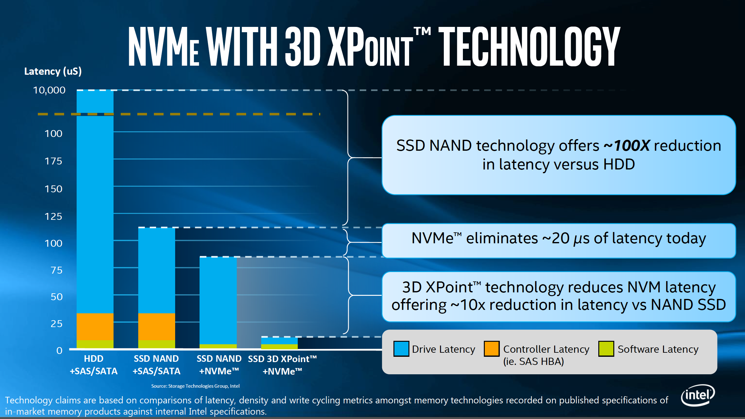
The interface is the key; connecting 3D XPoint via the NVMe interface brings a 10x reduction in latency compared to a standard NAND-based NVMe SSD. Utilizing other protocols, such as AHCI or SCSI, would saturate the CPU with computational overhead long before the system reaped the latency and performance rewards of the underlying medium.
Current page: What We Still Don’t Know
Prev Page New Details From IDF Next Page Other Things We’ve Wondered About…-
JeanLuc Is there any danger of you guys ever fixing how viewers enlarge pictures on your site?Reply
Seriously I don't know how many times I've commented on this issue but it seems to fall on deaf ears and given this is meant to be one of the larger tech site it's even more absurd. -
Bartendalot Very well written piece.Reply
Seems like it could be positioned as part of the purely platform as a future proofing connector.
While I don't think we will see true consumer products until 2018 at the earliest, are we looking at the main disruptive tech of the 10nm platform, or later?
The pressure coming from other market segments might give Intel a reason to get this out quickly. -
megiv The most important number is missing : Expected price per GB. I mean, they must have this number roughly already, or else they wouldn't go public with such big announcementsReply -
PaulyAlcorn ReplyThe most important number is missing : Expected price per GB. I mean, they must have this number roughly already, or else they wouldn't go public with such big announcements
I agree, it is the most important number! IMFT is merely saying that it will be between the price of NAND and DRAM, which gives them plenty of wiggle room - and isn't specific at all. -
Eggz I think this is going to be the kind of storage tech upgrade that will have a perceived impact akin to that of the HDD --> SSD tech upgrade - except better. The capacity decrease we felt when switching to SSDs was much more dramatic than that stated in the materials for Xpoint. I really hope it comes to market soon, but this time with a more attractive set of purchase options than early SSDs did.Reply -
Achoo22 I thought the trend of putting a capital X in a product title in hopes of catching the attention of the hipster crowd died away at the turn of the millennium. Will this product be compatible with XP running on Xtreme Xaggerated Xenthusuiast hardware?Reply -
kancaras Reply10X denser M.2 that's also 1000X faster? My dreams are coming true!
its 10x denser than dram, not nand, nand is also 10x denser than dram. i wouldnt expect affordable ssds with 3d Xpoint anytime soon. maybe cheaper but abit slower ram?
-
turkey3_scratch Reply16749024 said:Is there any danger of you guys ever fixing how viewers enlarge pictures on your site?
Seriously I don't know how many times I've commented on this issue but it seems to fall on deaf ears and given this is meant to be one of the larger tech site it's even more absurd.
Just right-click on the image and select "open image in new tab" to see it in full. -
SteelCity1981 looks like high speed storage is about to get a lot cheaper with xpoint if it can hold a lot more capacity than DRAM. might end of being the final nail in the coffin for HDD.Reply

