Intel-Micron 3D XPoint At Xroads
Today we're sorting out what's happened with Intel and Micron's 3D XPoint collaboration since it was announced in late July.
Get Tom's Hardware's best news and in-depth reviews, straight to your inbox.
You are now subscribed
Your newsletter sign-up was successful
The Stage Is Set
All is quiet on the non-volatile memory front these last few weeks. Intel-Micron dropped the 3D XPoint bomb in late July, which led to anticipation and speculation prior to the Flash Memory Summit. FMS proved to be a hotbed of speculation, which led to more anticipation ahead of the Intel's Developer Forum (IDF), which led to a great deal of talk, but very little new information.
Looking back, some nuances emerged, some details were clarified and some answers shrunk further into obscurity. We'll try to pick through what we heard, what we know and even what we don't know in an attempt to provide some closure before products begin to show up, or more details slip and slide into our hands.
Everyone seems to agree that 3D XPoint will be the sliced bread of 2016 and beyond, but nobody seems to know if we’re talking Ciabatta or Focaccia (to butcher the analogy).
Article continues belowIntel put its NVM solutions group GM Robert Crooke on stage at IDF with Al Fazio, an Intel fellow. Together they deftly dodged every detailed, how-it-works question tossed their way, leaving some audience members visibly bewildered. Geof Findley, Intel’s Director of Memory Ecosystems, practically dared his audience to ask questions about 3D XPoint, and himself to answer them; he half cringed, half laughed when he got to that small section of his presentation (on memory).
We also had a chance to chat with Crooke one-on-one. What follows is a summary of what we learned and what we didn't, along with a few tidbits that go beyond the singular topic of 3D XPoint (pronounced 3D cross-point).
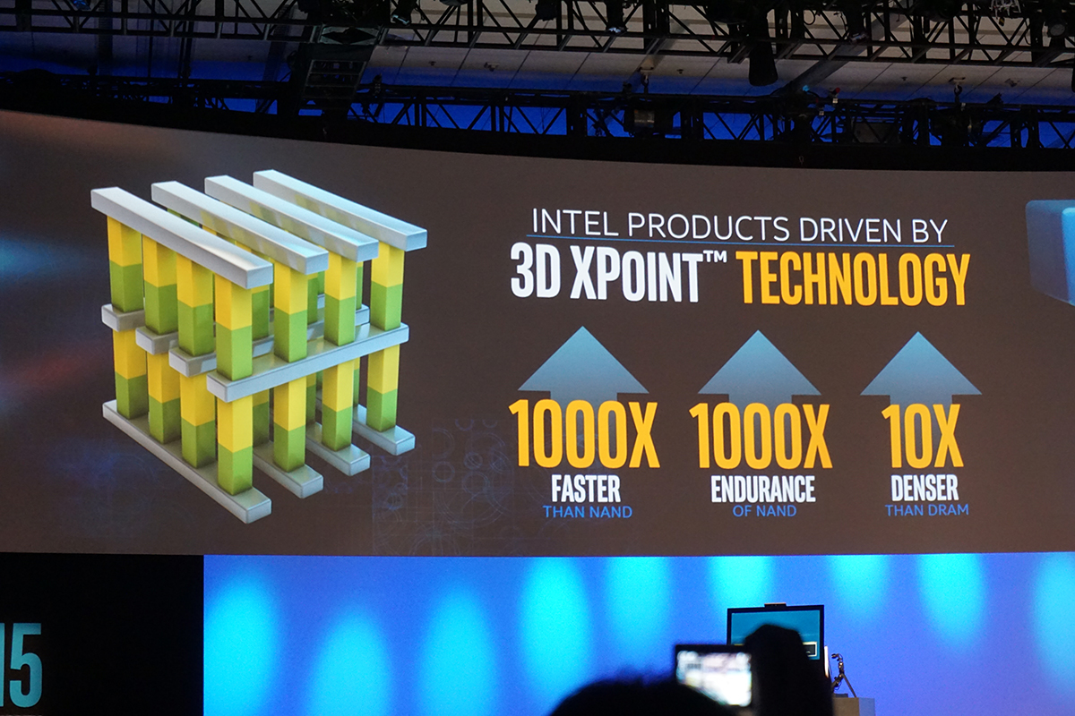
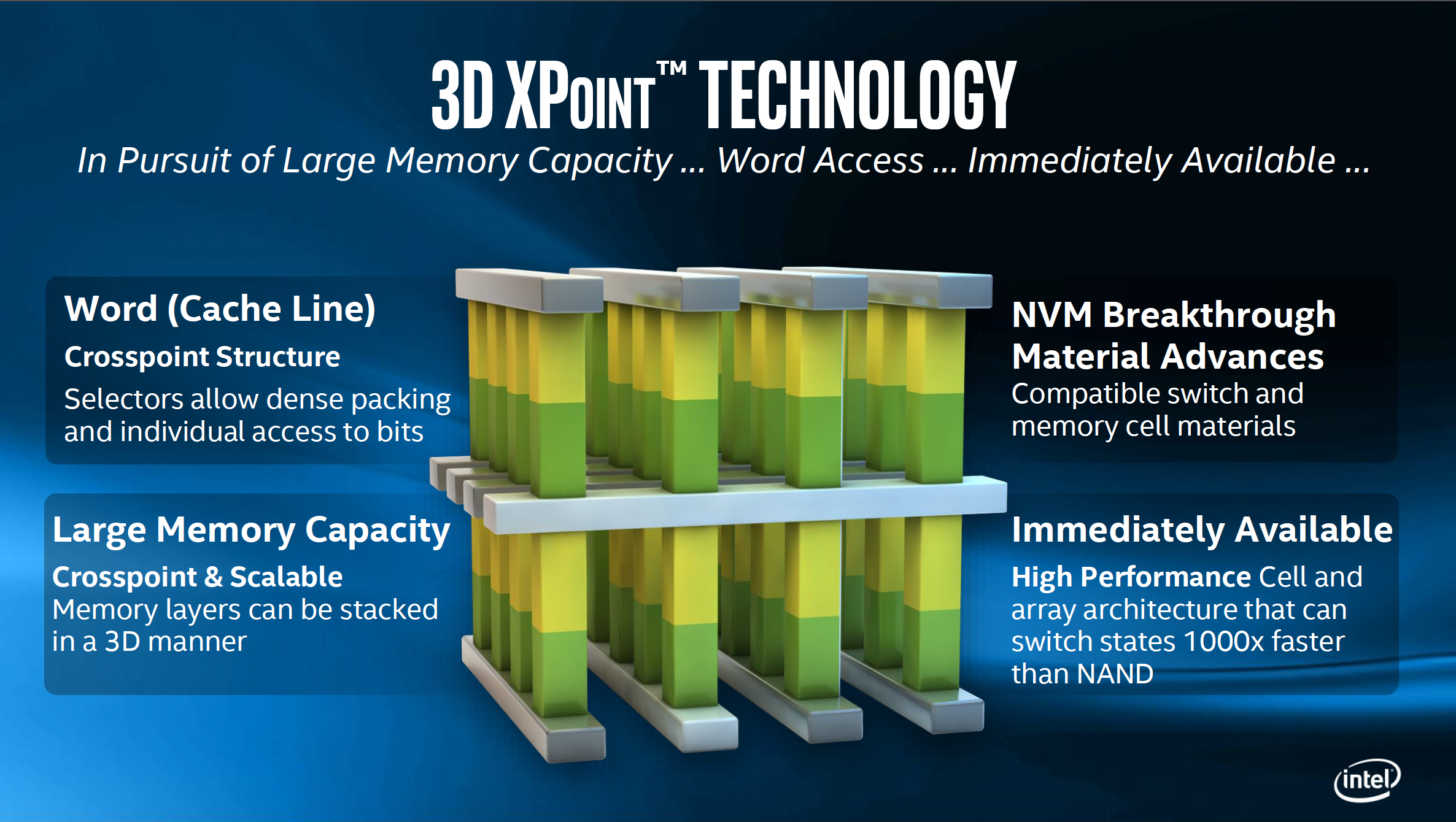
Here was our original piece the day of the Intel-Micron joint announcement. Back then, we learned the structure of 3D XPoint, we saw the models and we heard the explanation. Simply put, 3D XPoint is an intermediary storage layer between NAND and DRAM that offers 1000 times more speed and endurance than NAND along with 10 times the density of DRAM. To top it off, it is persistent, meaning it doesn't lose data when power is removed.
At FMS, we actually saw someone use their arms to re-create the 3D XPoint model (the one in the picture above) in a pantomimed form of solo Twister. One arm was the word line, the other the bit line, and the presenter made his head the memory cell. You get the picture (we didn’t have the foresight to have a camera ready for such a spectacle).
Get Tom's Hardware's best news and in-depth reviews, straight to your inbox.
At IDF, Intel had a gigantic 3D model on stage. We learned during the original announcement that Intel is building its first 3D XPoint iteration on the 20nm process with a 128Gb die density, and that there will initially be two layers. The technology could be scaled by stacking layers higher, and eventually by shrinking lithography.
We learned that 3D XPoint used a bulk material property change (rather than a stored charge) to address each cell. This provides a level of granularity we haven’t seen before, and subsequently offers better scalability and higher performance. However, we didn’t learn what that material change process would be.
MORE: Best SSDs For The Money
MORE: How We Test HDDs And SSDs
MORE: All Storage Content
-
JeanLuc Is there any danger of you guys ever fixing how viewers enlarge pictures on your site?Reply
Seriously I don't know how many times I've commented on this issue but it seems to fall on deaf ears and given this is meant to be one of the larger tech site it's even more absurd. -
Bartendalot Very well written piece.Reply
Seems like it could be positioned as part of the purely platform as a future proofing connector.
While I don't think we will see true consumer products until 2018 at the earliest, are we looking at the main disruptive tech of the 10nm platform, or later?
The pressure coming from other market segments might give Intel a reason to get this out quickly. -
megiv The most important number is missing : Expected price per GB. I mean, they must have this number roughly already, or else they wouldn't go public with such big announcementsReply -
PaulyAlcorn ReplyThe most important number is missing : Expected price per GB. I mean, they must have this number roughly already, or else they wouldn't go public with such big announcements
I agree, it is the most important number! IMFT is merely saying that it will be between the price of NAND and DRAM, which gives them plenty of wiggle room - and isn't specific at all. -
Eggz I think this is going to be the kind of storage tech upgrade that will have a perceived impact akin to that of the HDD --> SSD tech upgrade - except better. The capacity decrease we felt when switching to SSDs was much more dramatic than that stated in the materials for Xpoint. I really hope it comes to market soon, but this time with a more attractive set of purchase options than early SSDs did.Reply -
Achoo22 I thought the trend of putting a capital X in a product title in hopes of catching the attention of the hipster crowd died away at the turn of the millennium. Will this product be compatible with XP running on Xtreme Xaggerated Xenthusuiast hardware?Reply -
kancaras Reply10X denser M.2 that's also 1000X faster? My dreams are coming true!
its 10x denser than dram, not nand, nand is also 10x denser than dram. i wouldnt expect affordable ssds with 3d Xpoint anytime soon. maybe cheaper but abit slower ram?
-
turkey3_scratch Reply16749024 said:Is there any danger of you guys ever fixing how viewers enlarge pictures on your site?
Seriously I don't know how many times I've commented on this issue but it seems to fall on deaf ears and given this is meant to be one of the larger tech site it's even more absurd.
Just right-click on the image and select "open image in new tab" to see it in full. -
SteelCity1981 looks like high speed storage is about to get a lot cheaper with xpoint if it can hold a lot more capacity than DRAM. might end of being the final nail in the coffin for HDD.Reply


