


Imaging (Forming The Conductor Pattern), Continued
The (positive) Photoresist is made of a light sensitive material that dissolves when it is illuminated and developed (negative photoresist dissolves in the development process if it has not been illuminated). There are many ways to apply the Photoresist material onto the copper surface, but the most common is to heat and roll on a film containing the Photoresist material (referred to as Dry Film). It could also be sprayed on as a liquid, but the Dry Film offers higher resolution, resulting in thinner wires.
The mask is just a photo plot of the layer that is to be made. When this mask is placed over the photoresist before it is exposed with UV light, it prevents certain areas of the photoresist to be illuminated (assuming a positive photoresist). The copper covered by the photoresist in these areas is later turned into wires in the conductor pattern.
After the photoresist is developed the copper that is to be etched away is left uncovered. The etching is done by either lowering the board in an etching solution, or spraying the etching solution onto the board. Common chemicals for the etching solution are Ferric Chloride, Alkaline Ammonia, Sulfuric Acid + Hydrogen Peroxide, and Cupric Chloride. When the etching is complete the remaining photoresist is removed. This is referred to as 'Stripping' the photoresist.
The figure below illustrates how the copper wires are formed.
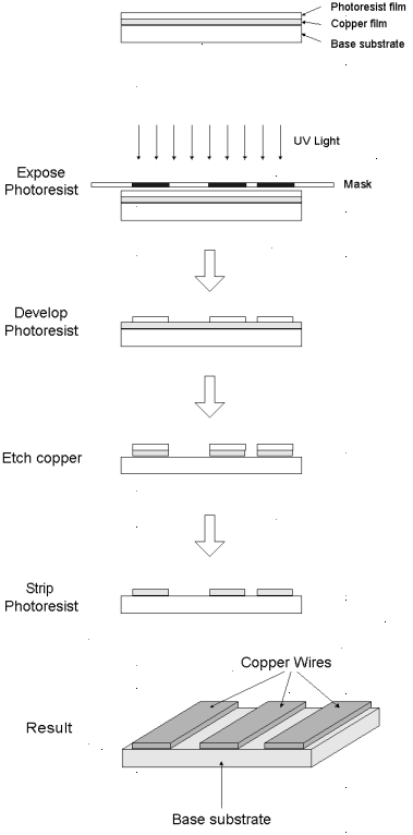
This process is done simultaneously on both sides of the board.