The Printed Circuit Board Primer
Get Tom's Hardware's best news and in-depth reviews, straight to your inbox.
You are now subscribed
Your newsletter sign-up was successful
Introduction
At the heart of the motherboards and graphics cards that we review on this site is the printed circuit board (PCB). On one side, you have the cold, hard facts and data of benchmarks and testing. On the other hand, you have the ingenuity of manufacturing, coupled with the artistry of designers. The PCB is an instantly recognizable symbol of both the beauty of electronics design, and its overwhelming sophistication. The following primer assumes no real knowledge of PCBs, but we've tried to keep it comprehensive, and go from A to B to create a general reference for all our readers.
What Is A PCB?
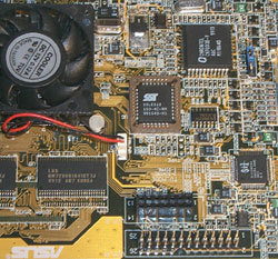
A PCB is found in almost every electronic device. If you have electronic components in a device, they are mounted on a PCB, big or small. Besides keeping the components in place, its purpose of a PCB is to provide electrical connections between the components mounted on it. As electronic devices have become more complex, and require more components, the PCB has become more populated, and dense with wiring and components.
Typical PCB. The bare board (without components) is also referred to as a 'Printed Wiring Board'.
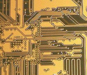
The substrate of the board itself is an insulating and non-flexible material. The thin wires that are visible on the surface of the board are part of a copper foil that initially covered the whole board. In the manufacturing process this copper foil is partly etched away, and the remaining copper forms a network of thin wires. These wires are referred to as the conductor pattern and provide the electrical connections between the components mounted on the PCB.
Conductor Pattern
Get Tom's Hardware's best news and in-depth reviews, straight to your inbox.

