The Printed Circuit Board Primer
Get Tom's Hardware's best news and in-depth reviews, straight to your inbox.
You are now subscribed
Your newsletter sign-up was successful
Multi-Layer Boards
To increase the area available for the wiring even more these boards have one or more conductor pattern inside the board. This is achieved by gluing (laminating) several double-sided boards together with insulating layers in between. The number of layers is referred to as the number of separate conductor patterns. It is usually even and includes the two outer layers. Most main boards have between 4 and 8 layers, but PCBs with almost 100 layers can be made. Large super computers often contain boards with extremely many layers, but since it is becoming more efficient to replace such computers with clusters of ordinary PCs, PCBs with a very high layer count are less and less used. Since the layers in a PCB are laminated together it is often difficult to actually tell how many there are, but if you inspect the side of the board closely you might be able count them.
The vias described in the section about double-sided PCBs always penetrate the whole board. When there are multiple layers of conductor patterns, and you only want to connect some of them, such vias waste space that could be used to route other wires. 'Buried ' and 'Blind ' vias avoid this problem because they only penetrate as many layers as necessary. Blind vias connect one or more of the inner layers with one of the surface layers without penetrating the whole board. Buried vias only connect inner layers. It is therefore not possible so see such vias by just looking at the surface of the PCB.
In multi-layer PCBs whole layers are almost always dedicated to Ground and Power. We therefore classify the layers as Signal, Power or Ground planes. Sometimes there is more than one of both Power and Ground planes, especially if the different components on the PCB require different supply voltages.
Technologies For Component Packing
Through Hole Technology
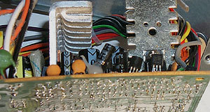
The components that are mounted on one side on the board while its legs are soldered on the opposite side are called 'Through Hole' (THT: Through Hole Technology). Such components takes up a large amount of space and require one hole to be drilled in the PCB for every leg. Hence, their legs occupy space on both sides of the board, and the connection points for them are also fairly large. On the other hand, THT components are fairly good mechanically connected to the PCB compared to Surface Mounted devices, which will be discussed below. Connectors for cables and similar devises also have to withstand mechanical stress and are usually THT.
Through Hole Components (soldered on bottom side)
Get Tom's Hardware's best news and in-depth reviews, straight to your inbox.
Current page: Multi-Layer Boards
Prev Page What Is A PCB? Continued Next Page Surface Mounted Technology