Tesla's wafer-sized Dojo processor is in production — 25 chips combined into one
Wafer-scale processors gain traction.

One of the less-noticed tidbits from last week's TSMC North American Technology Symposium was announcement that Tesla's Dojo system-on-wafer processor for AI training is now in mass production and is on track to be deployed shortly. More details about the giant processor were revealed at the event.
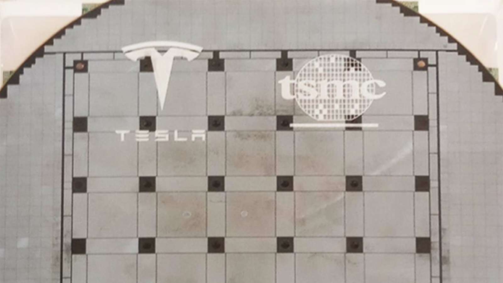
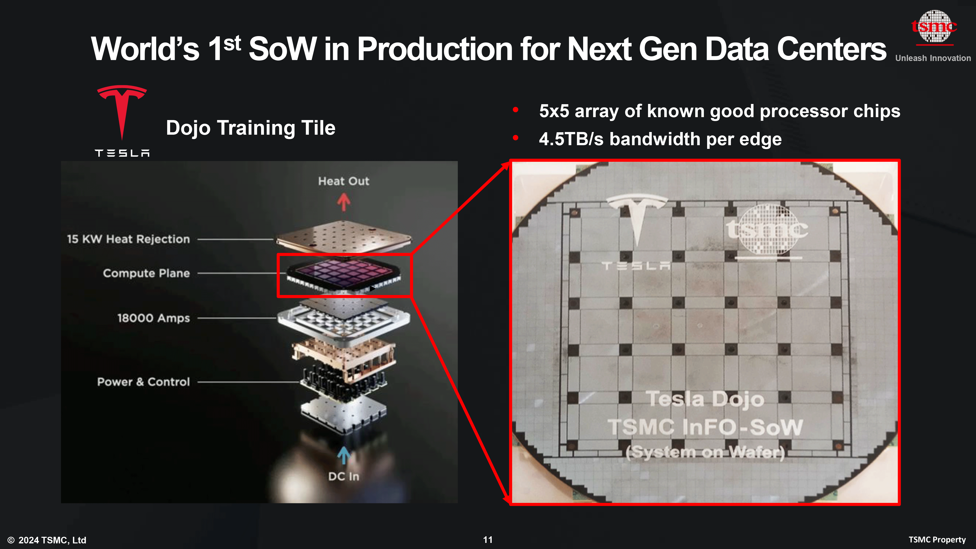
Tesla's Dojo system-on-wafer processor (or, as Tesla calls it, the Dojo Training Tile) relies on a 5-by-5 array of known good processor chips (which are reticle size, or close to that) that are placed on a carrier wafer and interconnected using TSMC's integrated fan-out (InFO) technology for wafer-scale interconnections (InFO_SoW). The InFO_SoW technology is designed to enable such high-performance connectivity that 25 dies of Tesla's Dojo would act like a single processor, reports IEEE Spectrum. Meanwhile, to make the wafer-scale processor uniform, TSMC fills in blank spots between dies with dummies.
Since the Tesla Dojo Training Tile essentially packs 25 ultra-high-performance processors, it is exceptionally power hungry and requires a sophisticated cooling system. To feed the system-on-wafer, Tesla uses a highly complex voltage-regulating module that delivers 18,000 Amps of power to the compute plane. The latter dissipates as much as 15,000W of heat and thus requires liquid cooling.
Tesla has yet to disclose the performance of its Dojo system-on-wafer — though, considering all the challenges with its development, it seems poised to be a very powerful solution for AI training.
Wafer-scale processors, such as Tesla's Dojo and Cerebras' wafer scale engine (WSE), are considerably more performance-efficient that multi-processor machines. Their main advantages include high-bandwidth and low-latency communications between cores, reduced power delivery network impedance, and superior energy efficiency. Additionally, these processors can benefit from having redundant 'extra' cores — or, in case of Tesla, known-good processor cores.
But there are inherent challenges with such processors for now. System-on-wafers currently have to exclusively use on-chip memory, which is not flexible — and, which may not be enough for all types of applications. This will be solved by the next-generation system-on-wafer platform called CoW_SoW, which will enable 3D stacking and installation of HBM4 memory on processor tiles.
For now, only Cerebras and Tesla have system-on-wafer designs. But TSMC is certain that, over time, more developers of AI and HPC processors will build wafer scale designs.
Get Tom's Hardware's best news and in-depth reviews, straight to your inbox.

Anton Shilov is a contributing writer at Tom’s Hardware. Over the past couple of decades, he has covered everything from CPUs and GPUs to supercomputers and from modern process technologies and latest fab tools to high-tech industry trends.
-
subspruce pipe dream lmao, did you know the last company that tried to make wafer-scale processing? Cerberas and they failed hard to make anything, yield is just too low for something that hugeReply -
bit_user Reply
LOL, where the heck did you hear that??subspruce said:pipe dream lmao, did you know the last company that tried to make wafer-scale processing? Cerberas and they failed hard to make anything, yield is just too low for something that huge
In fact, Cerebras achieved 100% yield of their WSE-2!
"Cerebras achieves 100% yield by designing a system in which any manufacturing defect can be bypassed – initially Cerebras had 1.5% extra cores to allow for defects, but we’ve since been told this was way too much as TSMC's process is so mature."
https://www.anandtech.com/show/16626/cerebras-unveils-wafer-scale-engine-two-wse2-26-trillion-transistors-100-yield
Do you honestly believe anyone smart enough to make a go of such an epic undertaking would be too naive to account for defects? Do you really think any VCs would provide enough funding to someone so naive that they could even afford to have a go at it?
Lastly, did you not read the part of the article where Tesla is pre-validating the chips they're stacking on the carrier wafer? That's another way to do it. -
ames61 Reply
To be accurate, that's no 100% yield if you sacrifice 1.5% cores and probably you have some other fault correction schemes to tackle D0. You can't avoid it.bit_user said:LOL, where the heck did you hear that??
In fact, Cerebras achieved 100% yield of their WSE-2!
"Cerebras achieves 100% yield by designing a system in which any manufacturing defect can be bypassed – initially Cerebras had 1.5% extra cores to allow for defects, but we’ve since been told this was way too much as TSMC's process is so mature."https://www.anandtech.com/show/16626/cerebras-unveils-wafer-scale-engine-two-wse2-26-trillion-transistors-100-yield
Do you honestly believe anyone smart enough to make a go of such an epic undertaking would be too naive to account for defects? Do you really think any VCs would provide enough funding to someone so naive that they could even afford to have a go at it?
Lastly, did you not read the part of the article where Tesla is pre-validating the chips they're stacking on the carrier wafer? That's another way to do it.
That said, WSE-2 has no significant sales\deployment and probably goes nowhere for other reasons. -
bit_user Reply
No, it's 100% yield because no wafers go in the trash bin. That's what yield actually means, not that there are zero defects.ames61 said:To be accurate, that's no 100% yield if you sacrifice 1.5% cores
How do you know? Cerebras is a private company. They're not obligated to report any of their sales or deployments.ames61 said:WSE-2 has no significant sales\deployment and probably goes nowhere for other reasons. -
ames61 Reply
By your definition even if you have only 30% working cores then you have 100% yield if you don't scrap a wafer. On this token, every process node which starts with, say 50% GDPW, has 100% yield.bit_user said:No, it's 100% yield because no wafers go in the trash bin. That's what yield actually means, not that there are zero defects.
How do you know? Cerebras is a private company. They're not obligated to report any of their sales or deployments. -
bit_user Reply
The reason I used the term "wafer" is that their product is an entire wafer. If we're talking about a normal chip, where you have multiple of them per wafer, then 100% yield would mean that all of your chips are working to spec. If you incorporated enough redundancy into your design, then you get higher yield.ames61 said:By your definition even if you have only 30% working cores then you have 100% yield if you don't scrap a wafer.
GPUs are a good example of this, where the the big ones ship with some functional units disabled. That doesn't mean they didn't yield, just that the design was de-rated in order to increase the yield.
Of course, one can talk about other kinds of yields, like yield of individual cores, but I think the industry standard definition of yield is essentially the proportion of chips that are manufactured to usable quantity.
And yes, it makes sense to talk about the amount of redundancy needed to achieve a given yield, on a given process. However, now we're getting into the details rather than talking about that top-line figure. -
subspruce Reply
i stand correctedbit_user said:LOL, where the heck did you hear that??
In fact, Cerebras achieved 100% yield of their WSE-2!
"Cerebras achieves 100% yield by designing a system in which any manufacturing defect can be bypassed – initially Cerebras had 1.5% extra cores to allow for defects, but we’ve since been told this was way too much as TSMC's process is so mature."https://www.anandtech.com/show/16626/cerebras-unveils-wafer-scale-engine-two-wse2-26-trillion-transistors-100-yield
Do you honestly believe anyone smart enough to make a go of such an epic undertaking would be too naive to account for defects? Do you really think any VCs would provide enough funding to someone so naive that they could even afford to have a go at it?
Lastly, did you not read the part of the article where Tesla is pre-validating the chips they're stacking on the carrier wafer? That's another way to do it. -
Joe Physics I can see no physicist posted here.Reply
Power = Voltage Times Current =
1.2v TSMC times 18,000 amps = 21,600 watts, not 15,000 watts.
The announcement is a bit phony. -
HotSlaw Why is putting chips on a wafer and using a semiconductor as the interconnect better than using say a decent conductor like copper. I could understand if it was all contained on the wafer and not having to deal with connections but it seems like that is lost when placing the silicon on top of another silicon that goes to another piece of silicon. Is there some type of length reduction happening here? Less metalization layer??Reply -
Joe Physics Reply
Silicon has the same coefficient of expansion as silicon. A copper substrate would expand at a different rate and may have issues.HotSlaw said:Why is putting chips on a wafer and using a semiconductor as the interconnect better than using say a decent conductor like copper. I could understand if it was all contained on the wafer and not having to deal with connections but it seems like that is lost when placing the silicon on top of another silicon that goes to another piece of silicon. Is there some type of length reduction happening here? Less metalization layer??

