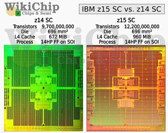
IBM z15 Almost Doubles Cache Density, Features 960MiB L4 eDRAM
IBM throws some cash at compute problems

As reported by respected chip analysis site WikiChip, IBM has detailed its latest z15 mainframe at the recent ISSCC conference. It has double the eDRAM cache density of its predecessor, despite being manufactured on the same process node. The z15 packs almost 1GB of L4 cache using a high-density eDRAM cell.
WikiChip has provided an overview of the changes. With 12.2 billion transistors, the z15 packs 2.5 billion more transistors than the z14, but the die size remains identical at 696mm2. This has allowed the L4 cache to be upgraded from 672MiB to 960MiB. The process node is also unchanged, utilizing a custom 14nm FinFET on SOI process co-developed with GlobalFoundries.
This process features an ultra-high-density eDRAM cell. With a cell size of 0.0174μm², it is even denser than TSMC’s densest 5nm SRAM bitcell of 0.021μm². Although this is not entirely surprising as SRAM typically uses six transistors, compared to one transistors and one capacitor in DRAM.
Article continues belowMore surprisingly, it has almost twice the density of its previous cell in the z14, which allowed the die size to remain unchanged. As WikiChip analyst David Schor describes:
“It turns out that by now, their 14 nm node is pretty good and there are decent overhead margins on the bitlines and wordlines. Tinkering with their z14 cells, they were able to double the bitline and wordline lengths within those margins.”
This allowed the number of sub-arrays to be halved to eight, using blocks of 2MiB instead of 1MiB previously. This reduced the I/O overhead and increased density by 30%. Power delivery changes accounted for another 38%, according to WikiChip, making for a total improvement in effective cache density of 80% higher MiB/mm2.
The L1 and L2 caches consist of SRAM cells and run at 5.2GHz, the L3 and L4 eDRAM caches run at 2.6GHz.
Get Tom's Hardware's best news and in-depth reviews, straight to your inbox.
Be sure to head over to the WikiChip article for fine-grained analysis of IBM's latest advancement.
