Intel Scales Neuromorphic Loihi to 64 Chips, 8 Million Neurons
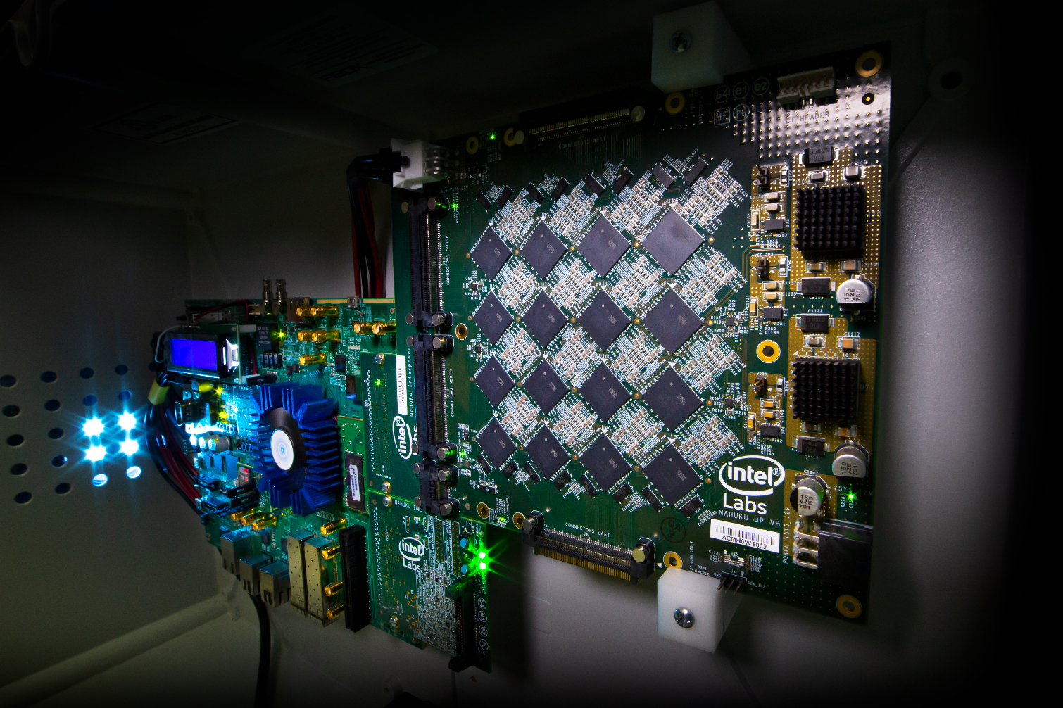
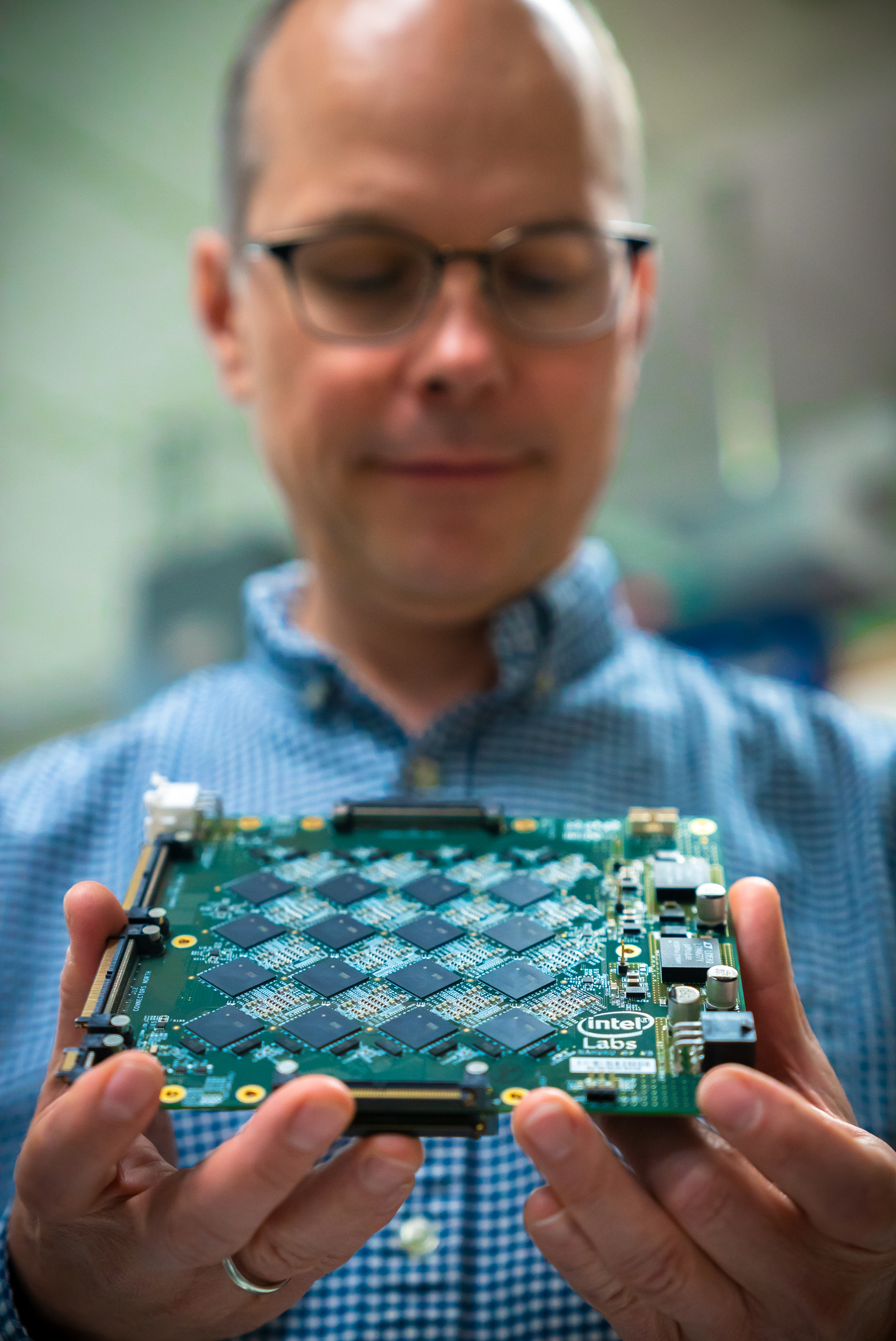
Intel today is announcing and making available to the broader research community an 8 million neuron system comprising 64 of its Loihi neuromorphic chips, codenamed Pohoiki Beach. Intel is aiming to scale Loihi further to 100 million neurons and 100 billion synapses by the end of the year. This marks a new milestone towards the eventual commercialization of the technology, as Intel has stated for the first time explicitly.
As a brain-inspired neuromorphic chip, Loihi is one of the rare designs that is not based on the von Neumann computing model. Its other unusual feature is that it is an asynchronous circuit, meaning that it does not have a global clock signal. More specifically, it implements an asynchronous spiking neural network (SNN).
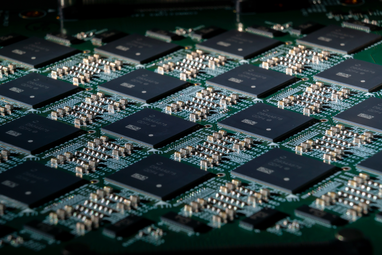
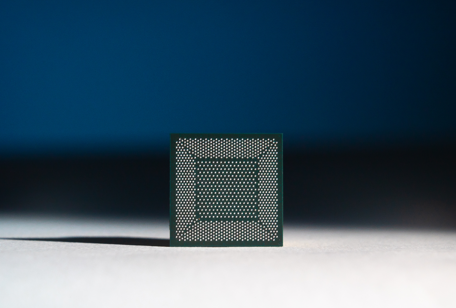
Other specs of the 128-core 14nm chip include 130,000 neurons and a thousand times as many synapses, three Quark x86 cores, 2.1 billion transistors and a die size of 60mm2. The Loihi programming toolchain includes a Python API. Intel says it is up to 1,000 faster and 10,000 times more efficient than CPUs for target applications that include sparse coding, graph search, path planning, simultaneous localization and mapping (SLAM) and constraint-satisfaction problems.
While the previous, USB form factor Kapoho Bay was still a single chip, Intel’s roadmap consisted of scaling up Loihi to a multi-chip system. Theoretically, Loihi can be scaled up to 16,384 chips – over two billion neurons (humans have ~86 billion neurons). While Intel has no plans to do such, in May 2018 Intel said that it saw a path to reach 100 million neurons in a single system by the end of 2019. If we assume that means a 768-chip system; it would contain over 1.5 trillion transistors.
With the current announcement of Pohoiki Beach today, Intel has scaled up Loihi to a 16-chiplet system, resulting in 8 million neurons, 3,840mm2 total die area, and 132 billion transistors. Pohoiki Beach is now available to the over 60 INRC ecosystem partners.
Intel has also provided several examples of how researchers use Loihi to prove the viability of neuromorphic computing. Projects include providing adaptation capabilities to a prosthetic leg, object tracking, automating a foosball table, learning to control an inverted pendulum and inferring tactile input to the skin of a robot.
Providing some benchmark numbers, Chris Eliasmith, co-CEO of Applied Brain Research and professor at the University of Waterloo, said: “With the Loihi chip we've been able to demonstrate 109x lower power consumption running a real-time deep learning benchmark compared to a GPU, and 5x lower power consumption compared to specialized IoT inference hardware. Even better, as we scale the network up by 50x, Loihi maintains real-time performance results and uses only 30 percent more power, whereas the IoT hardware uses 500 percent more power and is no longer real-time.”
Get Tom's Hardware's best news and in-depth reviews, straight to your inbox.
The system that Intel will use to reach 100 million neurons by the end of the year is codenamed Pohoiki Springs. The goal of these research systems is to clarify what application areas neuromorphic computing is most suitable for, to quantify how large the achievable gains are and pave the way for commercial use.
Intel announced Loihi in September 2017 and has since passed several milestones towards eventual commercialization. The chip came back from the fab in November 2017 and ran a test program. In March 2018, Intel created the Intel Neuromorphic Research Community (INRC) to spur innovation in neuromorphic computing with research into areas such as neuromorphic theory, programming models, SNN algorithms and applications to solve real-world problems. The company also provided community member access to a Loihi test system via the cloud. Last October, Intel held its inaugural INRC symposium, announcing fifty projects from over a dozen universities, and also made the chip available to its INRC partners via the USB form factor device Kapoho Bay.
-
bit_user Another great article, Arne.Reply
This is one of the more exciting recent developments in AI, IMO. For me, it recalls the Ni1000 that Intel co-developed, 25 years ago. It was not only asynch, but also analog, IIRC.
https://en.wikipedia.org/wiki/Ni1000 -
Growle Is it efficient enough that heat isn't an issue? I'm not too knowledgeable on this type of chip and am assuming its heat is low enough that passive cooling is enough.Reply -
bit_user Reply
The article says a GPU uses 109x the amount of power, for inferencing. According to the Intel press release, that's based on this paper:Growle said:Is it efficient enough that heat isn't an issue? I'm not too knowledgeable on this type of chip and am assuming its heat is low enough that passive cooling is enough.
https://arxiv.org/abs/1812.01739 (PDF: https://arxiv.org/pdf/1812.01739.pdf )
...which compared it to the GK106-based Nvidia Quadro K4000, among other things. That's a suspicious choice, since it's essentially a down-clocked GTX 650. And the paper was published in December 2018, after not only the Maxwell and Pascal series, but also the Turing GPUs had been released. So, either the researchers were specifically trying to make the Intel chip look as good as possible, or they literally just used an old GPU they happened to have lying around. Either way, it's pretty lame to compare a 28 nm GPU from 2013, with no optimizations for deep learning, to a purpose-built 14 nm ASIC.
Pascal is much more efficient (I'm going to guess about 3x or more, if you're using it's int8 support) and Turing's Tensor cores add another multiple somewhere in the single digits. So, if they did an honest comparison with like a Tesla T4, they'd struggle to get even 10x efficiency advantage.
Anyway, getting back to your question about absolute power consumption, you'll find that paper quotes the dissipation of a single chip at 0.110 W. Multiply that by 64 and you get about 7 W. So, no need for pesky heatsinks. -
bit_user I just noticed they used a batch size of 1, for that data! GPUs are much faster and more efficient with large batch sizes, as the paper subsequently acknowledges. When they increase the batch size to 64, the GPU gets a 47x speedup (it was already 2.6x as fast as Intel's Loihi chip, to begin with), while being about 50x as efficient as batch size 1! So, that cuts Intel's efficiency benefit to a mere ~2x, unless you have some sort of workload that absolutely cannot be batched (e.g. realtime/embedded control). Once you add the efficiency gains of Pascal or even Maxwell, their massive efficiency advantage should completely fall away. And we haven't even gotten to Turing's Tensor cores.Reply
BTW, the GPU is so slow that it's even outrun by their Xeon E5-2630 CPU! They don't say which version, but I'm guessing v3 or v4, which would have AVX2. Worse, that GPU is only about 2x the speed of the Jetson X1 SoC, which is essentially what powers the Nintendo Switch. So, we're talking about a really crap GPU.
Maybe I'll give the paper a full read, and post up anything more I find. So far, what sounded like a very promising development now seems like a PR whitewashing exercise.


