LCD Or Plasma - What's Your Pleasure? Understanding Modern Flat-Panel TV Technologies
A Little Lithography
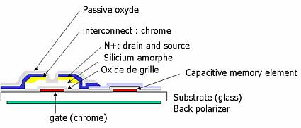
The process of fabrication of TFTs is very similar to the one used for the semiconductors we're familiar with.
A layer of chromium is deposited on a glass substrate to serve as the metallic grid for the transistors and storage capacitors. Then a thin layer of silicon oxide is deposited for the gate and storage-capacitor dielectric. A deposit of amorphous silicon is used to create a channel for the transistor. Two zones are then doped N+ to create the drain and the source. Finally, a metallic interconnection layer is deposited in order to connect the transistor (at left) to the storage capacitor (at right). This layer also provides the connection to the metallic data bus. The chromium grid, connecting all the transistors in a given line, will serve as the horizontal address line. Finally, the entire assembly is coated with a passivation oxide to protect the components.
Since amorphous silicon transistors are very poor compared to transistors on a doped substrate, a negative voltage (-5 V) applied to the grid ensures that the transistor is open (off). Once the transistor layer is deposited, the liquid crystal can be added.
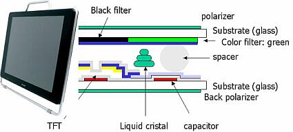
A spacer is added in order to keep the two glass plates from being pushed together. Then the liquid crystal is deposited, followed by an ITO electrode that serves as the reference electrode. Then come the color filters (green in our example), the front glass plate and another polarizer, oriented perpendicularly to the first one.
Above the transistor, a black color filter is deposited. The reason for this is simple: above the transistor, the voltage is not controlled in relation to the common electrode. It depends on the voltage in the data line, which can change even if this particular pixel isn't being addressed. So this poorly-defined area is masked to avoid discomfort for the user.
Get Tom's Hardware's best news and in-depth reviews, straight to your inbox.
Current page: A Little Lithography
Prev Page Addressing LCD Matrices Next Page Advantages And Disadvantages Of LCDs
