The Mother of All CPU Charts Part 1
Socket 370: April 1998 To July 2001, Continued
Still, to use the Tualatin CPUs, a new chipset with so-called T-stepping was necessary. But it gets even easier: With some skill, a modification can be made so that the CPU can also be used in a conventional BX board. It looks like this in detail: Pins AN3, AK4 and AJ3 are isolated so that they have no electrical connection to the socket. In most motherboards it is necessary to connect Pin AK4 with AK26; a simple jumper does this with just a few motions. Now only pins AM34, AL35 and AL37 as well as AK36 are connected to one another.
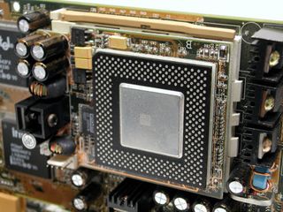
Adapters aplenty, even for Socket 8 to Socket 370
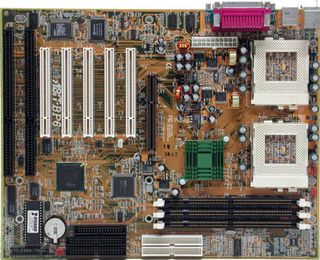
The popular BP6, which made possible the dual operation of Celeron CPUs with Mendocino core and BX440 chipset.

Intel Pentium III with Coppermine core on Socket 370. This had 9.5 million transistors for the processing unit and 18.6 million for the cache.
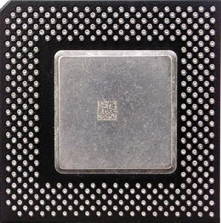
The Celeron with Mendocino core had extremely good overclocking potential.
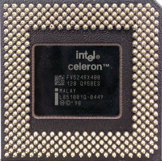
The back of the Celeron CPU (Mendocino), which did not have SSE, had a power loss of 28 Watts and was produced with 250 nm technology.
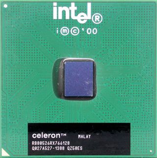
The Celeron with Coppermine core was available up to 1.1 GHz, with an FSB of either 66 or 100 MHz.
Stay on the Cutting Edge
Join the experts who read Tom's Hardware for the inside track on enthusiast PC tech news — and have for over 25 years. We'll send breaking news and in-depth reviews of CPUs, GPUs, AI, maker hardware and more straight to your inbox.
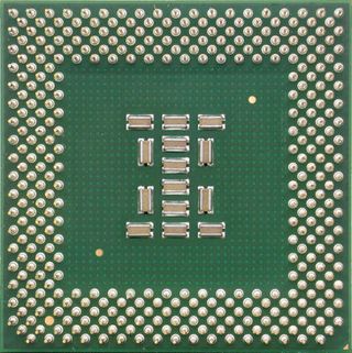
The back of a Pentium III CPU in organic packaging.
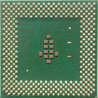
The back of the legendary Pentium III with Tualatin core. Even today, it is still being traded on the market.
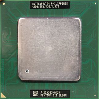
The Pentium III with Tualatin core marked Intel's transition to 130 nm technology as early as the days of Socket 7. The 1.4 GHz had a maximum power loss of 28 Watts.
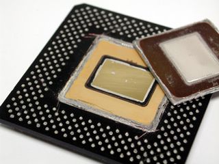
The Celeron with a removed head spreader
Current page: Socket 370: April 1998 To July 2001, Continued
Prev Page Socket 370: April 1998 To July 2001 Next Page Socket 370: April 1998 To July 2001, ContinuedTom's Hardware's dedicated news crew consists of both freelancers and staff with decades of experience reporting on the latest developments in CPUs, GPUs, super computing, Raspberry Pis and more.
-
Rare Intel Pentium P5 wafer with chips:Reply
http://www.chipsetc.com/intel-journey-inside-educational-chip-kits.html
Most Popular


