


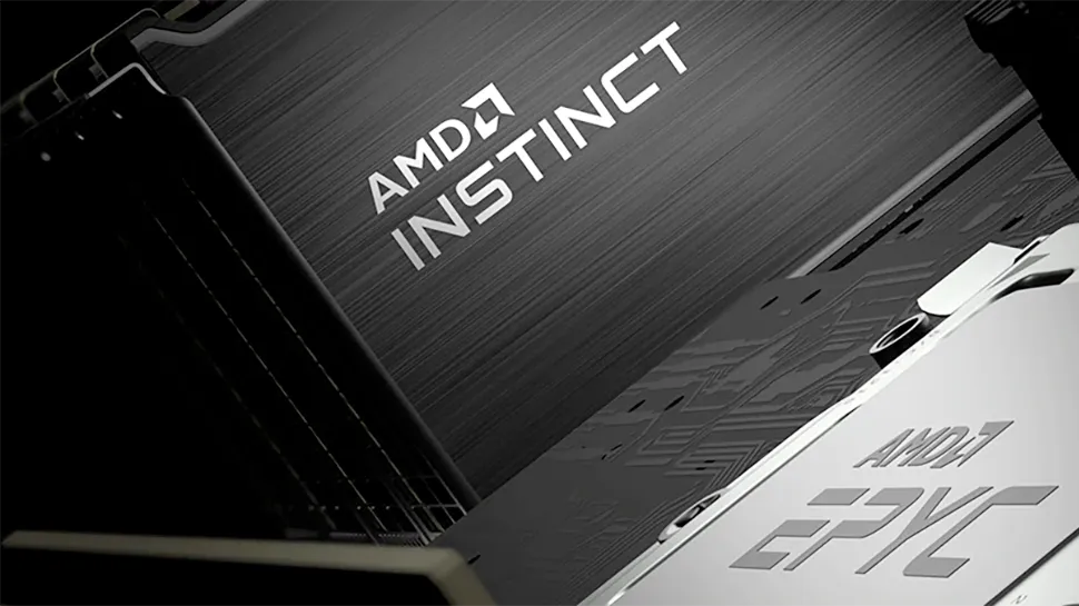
AMD is not going to talk about its next-generation Instinct MI200 compute GPU for a several months, but its Linux patches continue to disclose new features and capabilities of this upcoming products. As it turns out, the GPU that is set to used for the Frontier exascale supercomputer (to be delivered this year) will have a rather monstrous memory subsystem supporting up to 128GB of HBM2E DRAM.
We already know that AMD's Instinct MI200 compute GPU codenamed Aldebaran based on the CDNA 2 architecture uses two dies in a single chip package using AMD's Infinity high-performance interconnections. One of AMD's latest Linux patches for its AMD64 EDAC driver (which sits on top of system DRAM ECC) reveals memory architecture of the Instinct MI200, reports Phoronix.
As it turns out, each of Aldebaran dies has four unified memory controllers (UMCs). Each UMC supports eight memory channels, each channel is connected to 2GB of Gen 2 high-bandwidth memory (HBM2). While AMD's description of Aldebaran's memory subsystem is fairly detailed, it can actually cause some confusion, so let us try to explain things a bit.
An HBM2 stack supports a 1024-bit wide interface, which is typically called an HBM2 channel. However, internally, an HBM2 stack is comprised of two, four, or eight DDR DRAM devices with two 128-bit channels per device on a base logic die. Essentially, an HBM stack supports up to eight 128-bit channels over its 1024-bit interface.
At this point it is not completely clear what AMD means by a channel, but it looks likely that it means eight 128-bit DDR channels inside 1024-bit HBM2 stacks. Essentially, this means that each of Aldebaran's UMCs can connect to four HBM2 stacks over a 4096-bit memory interface. With each channel addressing 2GB of memory, one die can address up to 64GB of memory, whereas two dies can work with up to 128GB of memory. Actual bandwidth of Aldebaran's memory subsystem is unknown, but assuming that AMD uses SK Hynix's latest 3.6 Gbps HBM2 stacks, its memory subsystem will provide the GPU up to a whopping 3.64TB/s of bandwidth.
Compute GPUs have to use ECC for memory, so part of their memory bandwidth and capacity is used for error corrections. To that end, not all of Instinct's MI200's 128GB of memory will actually be available to applications.
AMD has not yet commented on Aldebaran.
The official description of Aldebaran's memory subsystem by AMD reads as follows:
Aldebaran has 2 Dies (enumerated as a MCx, x= 8 ~ 15)
Each Die has 4 UMCs (enumerated as csrowx, x=0~3)
Each die has 2 root ports, with 4 misc port for each root.
Each UMC manages 8 UMC channels each connected to 2GB of HBM memory.
