Die Shots of Apple's A14 Bionic & M1 SoCs Compared: Same Architecture, Different Goals
Reverse engineering analysts compare Apple's latest SoCs

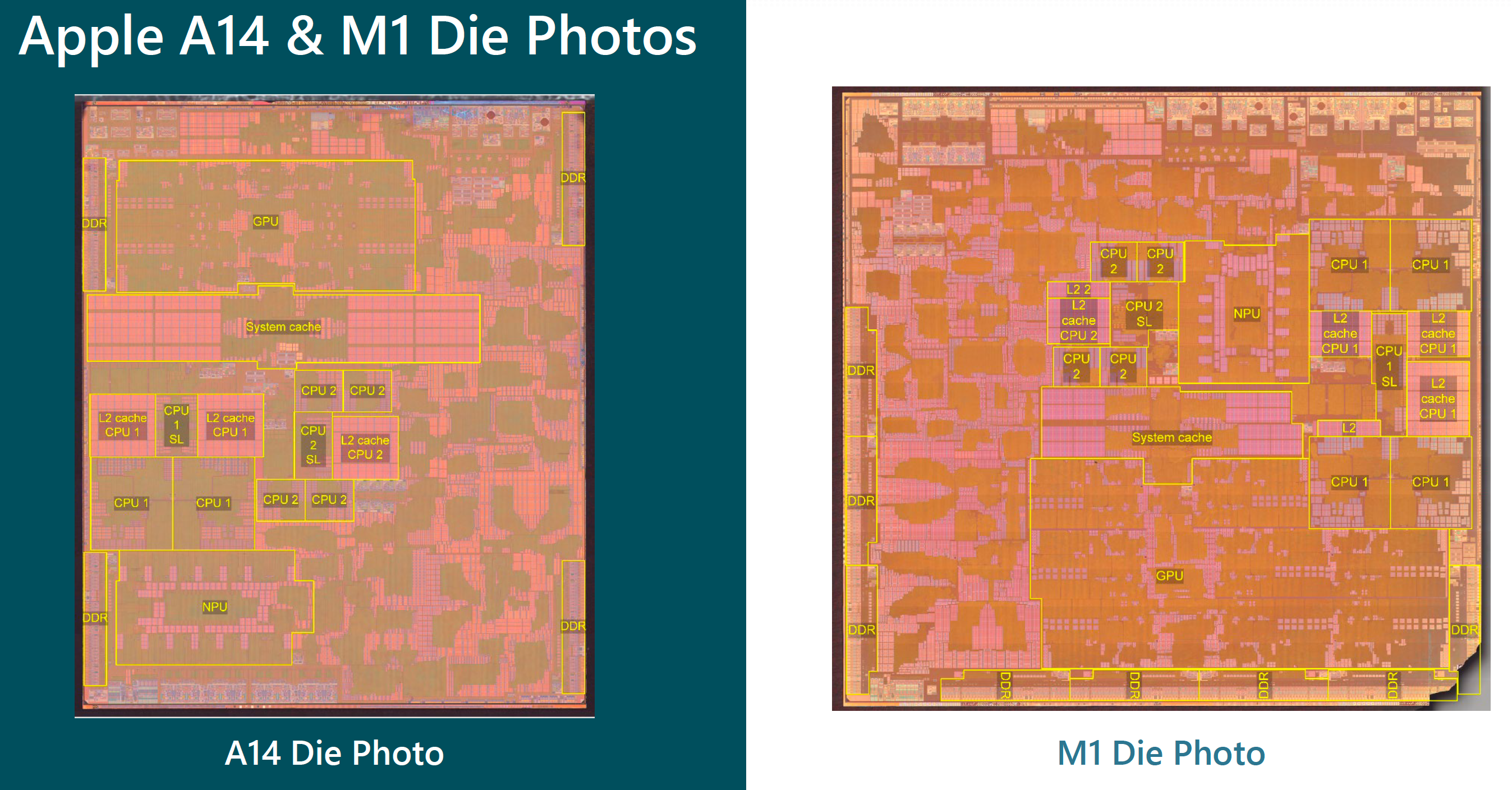
Detailed die shots of Apple's A14 Bionic and M1 system-on-chips published by TechInsights might reveal some additional information about SoCs from one of the most secretive industry giants.
The Big Transition Incoming
Without a doubt, Apple's launch of its own system-on-chips (SoCs) for Macs and its intention to transition its PCs to the Arm architecture is among the most important tech events of 2020. The company plans to completely stop using Intel processors inside its PCs in the coming years and is working on a series of Arm-based SoCs that will address everything from entry-level notebooks all the way to high-end Mac Pros desktops. The move not only means decoupling Apple from Intel (and to a large degree the rest of the industry that still relies on x86 and will continue to for at least a decade), but it will also demonstrate (or not) the company's ability to develop SoCs that are competitive with Intel's CPUs, as well as GPUs from companies like AMD and Nvidia.
Apple traditionally doesn't disclose many details about its hardware, so it isn't always easy to analyze its innovations and draw conclusions about where things are going. Fortunately, SoC floorplans expose some general ideas, and recently, advanced technical analysis and reverse engineering firms have released die shots of Apple's A14 Bionic and M1 SoCs, revealing some additional details about these processors. TechInsights seems to have the most detailed die shots available today, though other consulting firms have also published images of the die shots.
So Close Yet So Far
It's no secret that Apple's A14 Bionic and M1 have a lot in common. Apple makes them with the same TSMC N5 process technology, and they are very similar from an architectural standpoint (e.g., they are SoCs, they use a unified memory architecture) with the same Firestorm and Icestorm general-purpose CPU cores, the same NPU (neural processing unit) engine, and presumably the same GPU architecture.
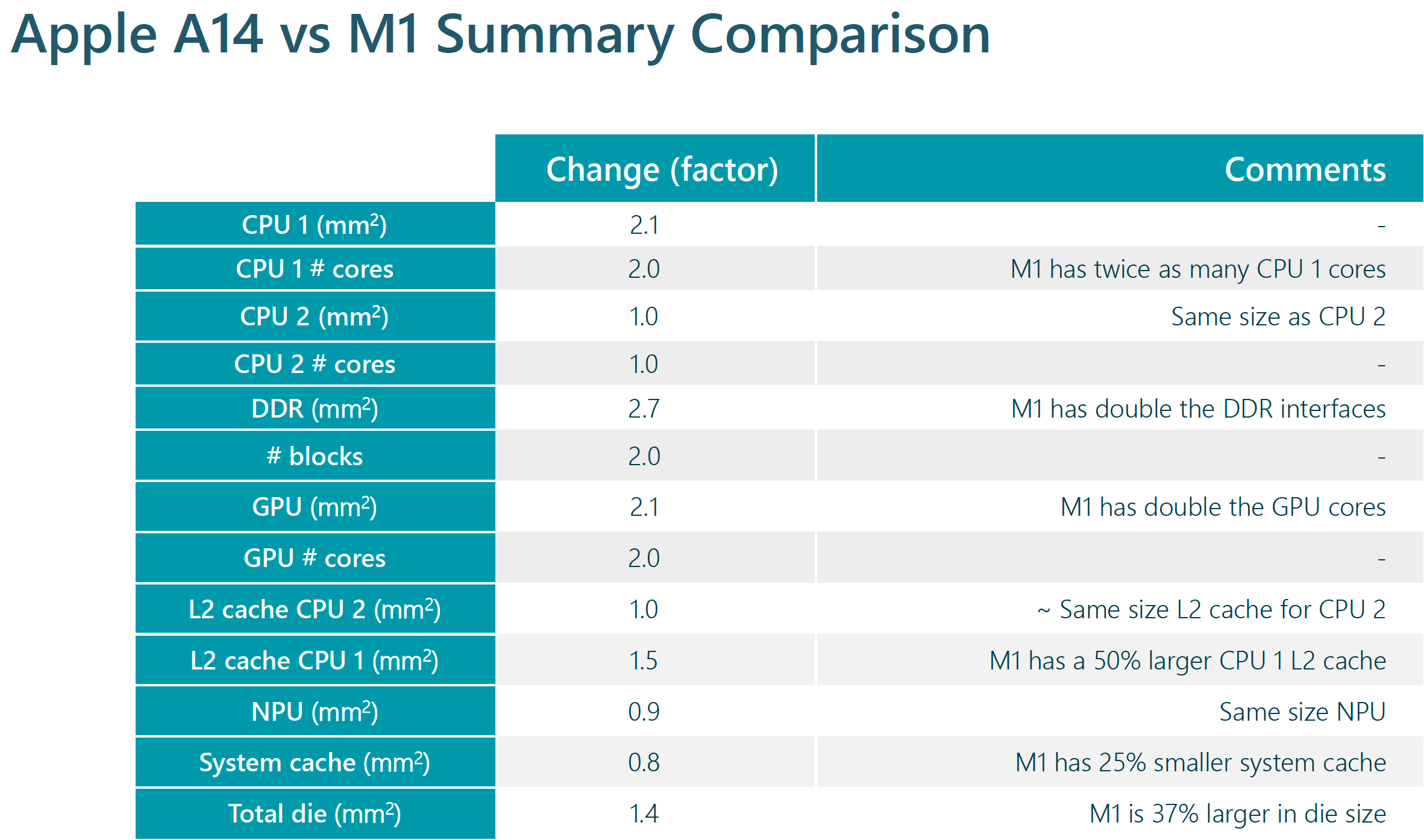
Being aimed at notebooks and compact desktops, Apple's M1 processor is designed to be faster than the A14 across the board. Yet, the M1 — which is 37% larger — is not exactly an A14 on steroids.
| Apple's A14 Bionic and M1 At a Glance | Header Cell - Column 1 | Header Cell - Column 2 |
|---|---|---|
| Row 0 - Cell 0 | A14 Bionic | M1 |
| Transistor Count | 11.8 billion | 16 billion |
| Die Size | 88 sq. mm | ~120.5 sq. mm |
| Genera-Purpose Cores | 2 FireStorm, 4 IceStorm | 4 FireStorm, 4 IceStorm |
| L2 Cache | ? | 12MB on FireStorm, 4MB on IceStorm |
| GPU Clusters | 4 | 8 (?) |
| NPU | 16-core NPU | 16-core NPU |
| Memory Interface | 64-bit LPDDR4X (4-channel) | 128-bit LPDDR4X (8-channel) |
The M1 packs more CPU cores than the M14: it comes with four high-performance Firestorm cores running at up to 3.20 GHz with enlarged caches to maximize single-thread performance by speeding up instruction and data access as well as reducing latency. The SoC also has four energy-efficient Icestorm cores with up to a ~2.0 GHz frequency. Apple doubled the number of Firestorm cores yet left the number of Icestorm cores intact, perhaps because the latter are less important in the PC space, and four is an optimal number. It is unclear from the floorplan whether Apple used any optimizations to make CPU cores run faster (e.g., use high-performance transistors instead of low-power ones for certain blocks). Still, there are arguments for implementing them and for not implementing them.
The M1's GPU is twice as large as the GPU on the A14, which demonstrates Apple's priorities to some degree, at least as far as PCs are concerned. The company likes graphics even though not all programs on Macs use GPGPU extensively. Apple has always been one of a few PC makers to use Intel's CPUs with beefy GPUs, so nothing changes with the transition to its own processors.
Get Tom's Hardware's best news and in-depth reviews, straight to your inbox.
To feed the more powerful CPU and GPU subsystems with enough data, the M1 uses a 128-bit eight-channel LPDDR4X-4266 memory subsystem (up from a quad-channel 64-bit memory subsystem in the A14). Apple also shrunk the system level cache by 25%, which is logical given that the memory subsystem became more powerful. It's noteworthy that Apple decided to continue using LPDDR4X memory and not transition to LPDDR5 to further boost memory bandwidth. Perhaps re-using the controller and PHY IP originally designed for smartphones is a cost-saving measure that reduces R&D expenses.
As far as the neural processing unit (the NPU) is concerned, the M1 and the A14 have identical 16-core units, which is not particularly surprising as modern AI workloads are projected to be generally similar both for smartphones and laptops.
TechInsights and other analysts cannot identify all of the M1's blocks. Still, it is generally believed that Apple's latest A14 and M1 SoCs feature numerous special-purpose accelerators to handle tasks specific to MacOS or various demanding workloads, such as media encoding/decoding. Considering that at least one-third of M1's floorplan cannot be identified, it is likely that Apple built a lot of custom blocks into the chip, including its famous T2 chip. Meanwhile, the M1 also features PC-specific interfaces, such as DisplayPort and Thunderbolt/USB 4.
Summary
Apple's M1 system-on-chip is an evolution of the A14 Bionic, a smartphone SoC, but with numerous optimizations designed specifically for smaller notebooks as well as compact desktops.
Overall, Apple's M1 promises at least twice the general-purpose performance, at least twice the graphics performance, and twice the memory bandwidth compared to the A14. All of this comes at the cost of a 37% larger die size. Keeping in mind that the M1 does not have to be as energy-efficient as the A14, its actual performance improvement could be tangibly higher, given its higher clocks and other possible optimizations. Furthermore, assuming that the M1 has numerous Apple-specific accelerators, we can expect it to be tangibly faster than Intel processors in some applications (for example, Apple ProRes RAW encoding/decoding).
Apple clearly designed its M1 for a particular set of products, notably the MacBook Air, MacBook Pro 13, and Mac Mini. These systems are hardly ever used for tasks that require truly high performance, which is perhaps why the company did not go beyond four high-performance cores in the design. Input/output capabilities of M1 are also moderate: the SoC has two display engines, it lacks native HDMI support, and it apparently only supports two USB 4/Thunderbolt ports.
In general, with its M1, Apple has designed an SoC that promises significantly higher performance than the M14 Bionic, but it only took 37% more die area to get there. The company optimized many elements of the design (e.g., added caches, higher clocks, a wider memory interface, PC-specific interfaces) to hit its PC performance targets, but left many other things intact (e.g., 16-core NPU, LPDDR4X memory support), which demonstrates a very rational approach to design and manufacturing costs.

Anton Shilov is a contributing writer at Tom’s Hardware. Over the past couple of decades, he has covered everything from CPUs and GPUs to supercomputers and from modern process technologies and latest fab tools to high-tech industry trends.
