Innosilicon, a contract designer of ASICs from China, has taped out the world’s first chip using Semiconductor Manufacturing International Corp.’s N+1 process technology, a 7 nm-class node for inexpensive chips. The tape out is a major breakthrough for Chinese domestic semiconductor industry in general as well as SMIC in particular as the company is trying to catch up with much bigger rivals like GlobalFoundries, Samsung Foundry, and market leader Taiwan Semiconductor Manufacturing Co. But will SMIC’s N+1 ever be used for mass production now that the company is in the U.S. Department of Commerce’s Entity List?
(Via cnTechPost, China Renaissance Securities, DigiTimes, EE Times, Innosilicon, IC Insights)
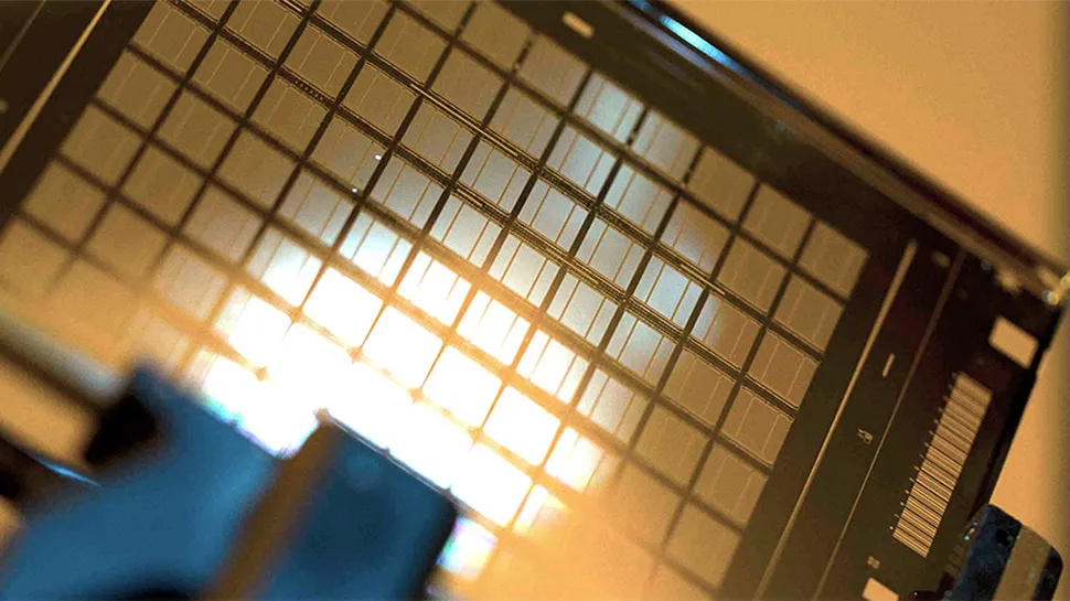
The Tape Out
Being a contract designer of ASICs and a provider of advanced IP, Innosilicon does not disclose whether the chip taped out using SMIC’s N+1 node was a test chip carrying various IP, or an actual commercial product ordered by one of Innosilicon’s clients.

What the company does say is that the chip underwent ‘multiple rounds of test iterations in the past few month’ to help SMIC to achieve viable yields and that the chip has passed ‘all the function tests passed in one stroke.’ Innosilicon also claims that it has invested ‘tens of millions of yuan in design optimization’ (¥10 million is about $1.49 million) since 2019 before the N+1 process was even announced.
Innosilicon and SMIC collaborated for years and the contract chip designer says that it has helped dozens of SMIC’s customers to develop chips using both mature (e.g., 55 nm, 40 nm, 28 nm) and FinFET-based process technologies (14 nm, 12 nm, 7 nm), so it is not particularly surprising that Innosilicon is the first company to try SMIC’s N+1.
Even if SMIC and Innosilicon have taped out the first commercial N+1 chip, it might take a year before that ASIC will be mass produced. In any case, the tape out means that at least some IP for N+1 is now available and Innosilicon knows how to use the technology.
SMIC’s N+1
SMIC’s N+1 fabrication technology is the company’s next major node that will follow the foundry’s 14 nm and 12 nm manufacturing processes.

According to SMIC, when compared to its 14 nm node, its N+1 technology can improve performance by up to 20% (at the same clocks and complexity) or reduce power by 57% (at the same power and complexity). In addition, the technology can potentially increase transistor density by up to 2.7 times (though not for all transistor structures).
While scalability and power consumption improvements of SMIC’s N+1 are significant (over its 14 nm node) and therefore the process can be compared with GlobalFoundries’s 12LP+, Samsung Foundry’s 8LPP, and even TSMC’s N7 (7 nm, non-EUV), its performance enhancements are modest at best. Therefore, SMIC itself positions N+1 primarily for low-power and low-cost devices.
Back in August, SMIC said that its N+1 had ‘finished customer product verification.’
Since SMIC has not received its TwinScan NXE extreme ultraviolet (EUV) scanner that it purchased from ASML back in 2018, its N+1 and N+2 technologies do not use EUV, unlike leading-edge processes from Samsung and TSMC. Relying purely on DUV lithography, significantly reduces SMIC’s ability to advance its nodes in terms of performance and scalability, so it will not be able to compete against market leaders in the leading-edge space any time soon.
For now, this is not a significant problem for SMIC as mature technologies (40/45 nm and thicker) accounted for 90.9% of its wafer revenue in Q2 2020. Meanwhile, 28 nm and 14 nm accounted for only 9.1% of the company’s wafer revenue in the second quarter with the former being considering more popular than the latter. But Chinese companies need advanced FinFET-based process technologies and many of them would prefer to work with a local supplier.
Rising Demand
There are a number of looming megatrends — 5G, AI, edge computing, and HPC — that will increase global demand for chips in the coming years. But in China there is an ongoing semiconductor boom. The number of local chip designers increased from 736 in 2015 to 1,780 in 2017, according to China Renaissance Securities.

All of these Chinese companies need to make their chips somewhere. In fact, Chinese fabless developers are expected to account for 22% of the global foundry sales in 2020, IC Insights believes. It remains to be seen how cease of shipments to HiSilicon affects foundry sales to China in the short and long-term future, but it is evident that the country is the second biggest consumer of foundry services after the USA.

Today, 67% of Chinese orders for logic chip production are served by TSMC, UMC, and GlobalFoundries in Taiwan, Singapore, and the USA. SMIC is China’s biggest and most advanced foundry that produces 19% of the chips the country needs, so it is logical for the company to keep developing leading-edge process technologies rather than refocusing on specialized nodes as it has a massive room for growth.

But there is a huge catch for SMIC.
The Entity List
Earlier this year the U.S. Department of Commerce threatened to include SMIC into its Entity List as it believes that the company serves needs of China’s People’s Liberation Army, something that SMIC denies it does. In addition, it tightened restrictions on technology exports to China, Russia, and Venezuela

As a result, if a U.S.-based company (or a company that develops or makes something in the USA) wants to sell production tools, parts, materials, software or something else to SMIC, it has to obtain a license from DoC, which is expected to review such license applications under a presumption of denial (at least before the Presidential election in November).
Consequently, it is close to impossible for SMIC to get advanced equipment, spare parts for existing tools, materials, and software it needs not only to keep developing new process technologies, but to maintain and expand current capacities.
Uncertain Prospects for N+1?
SMIC has been gradually increasing its CapEx for several quarters now as it has been investing in new facilities and equipment. Some analysts believe that SMIC’s N+1 and N+2 nodes rely on the same (or nearly the same) set of production tools that is used for the company’s 14 nm and 12 nm technologies.

Therefore, assuming that SMIC has stockpiled enough modern DUV scanners and other tools (as well as spare parts) to build sufficient capacity to compete against its bigger rivals, its N+1 and N+2 processes might have good chances to become relatively popular in the coming years. Meanwhile, neither N+1 nor N+2 nodes are going to be competitive with leading-edge nodes from other companies when they enter mass production in 2021 ~ 2023 timeframe.
Furthermore, even though SMIC has several R&D teams working on new fabrication processes, its roadmap looks increasingly uncertain as the company will be unable to adopt EUV lithography and GAAFET structures — the key enablers for next-generation nodes — for years to come.
Or Uncertain Future for SMIC?
But while EUV and GAAFETs are important for SMIC’s long-term future, the inclusion of the company into the Entity List brings a host of challenges that may force the company to change its plans dramatically, some analysts believe.

SMIC can get DUV scanners from ASML without any restrictions. Lithography tools are very important for production of semiconductors, but they are not the only tools used at a fab. There is equipment used for high-precision metrology, deposition, etching, photoresist stripping, and wafer cleaning that is made primarily by companies from the USA. There are alternative from Europe and Japan, but an insertion of a new tool always means a change of the whole flow, a lengthy and risky process. If the company fails to get one advanced tool or spare parts for it on time, this ruins its whole production flow. In the worst case scenario the company might need to halt production using its FinFET process technologies and retrofit its capacity for legacy nodes.
“We believe the build-up of spare parts/materials should keep SMIC’s operations afloat for 3-6 months, even if its US suppliers now need to get licenses before shipping, and the chance of a positive response is deemed low,” wrote Szeho Ng, an analyst with China Renaissance Securities, in a note to clients. “Our base case now assumes that its FinFET businesses will largely halt (given the high reliance on U.S. tech supply, and the strategic importance of the tech for making core chips in sensitive markets), with the installed capacity retrofitted for lower-ASP legacy 300-mm (28-90 nm nodes) manufacturing. 200-mm (130nm-and-above nodes) fabs will stay as business as usual, in our opinion.”
At present SMIC’s FinFET business probably accounts for 2% ~ 3% of the company’s revenue, so even if the company has to halt production using 14nm and cancel 12nm and N+1 plans, it is not going to suffer a significant sales drop. But advanced nodes tend to be profitable and attractive for big clients. Furthermore, retrofitting new fabs for older technologies will automatically bring net profits down (tools to be replaced have not depreciated yet, which means losses).
Overall, the analysts believe that SMIC’s future largely depends on the U.S. government’s attitude towards the company rather than on its own R&D expertise or manufacturing prowess.
“We see the U.S. government’s attitude towards SMIC as remaining the key to its destiny, as an imminent full decoupling of the company from the U.S. tech reliance (even for legacy 300-mm) may not be as easy as some industry watchers expect,” wrote Ng. “The U.S. tech influence goes beyond the equipment/materials areas, and goes further upstream to the EDA markets where the U.S.’s global dominance is even higher. Furthermore, it remains to be seen what the attitude of Japan may be, as it also plays a fairly important role in global equipment/materials supplies.”
