Hot Chips 34 Reveals Intel's 3D Foveros Ambitions for Meteor Lake, Arrow Lake CPUs
Symposium runs from August 21 to 23.
The organizers have shared the schedule for the Hot Chip Symposium 2022. Intel has booked a lot of presentation time with experts sharing information and insight about its latest GPUs, CPUs, foundry technologies, etc. Other key PC technology firms at Hot Chips 34 include AMD, Arm, and Nvidia. Well-known tech industry pioneers like Samsung, Tesla, MediaTek, and Cerebras will be there. Due to the ongoing pandemic situation, Hot Chips 34 will be a virtual conference that will take place live over the days specified. Still, all presentations will be recorded and made available after processing.
Intel's Hot Chips 34 Schedule
- Intel’s Ponte Vecchio GPU: Architecture, System and Software. Monday, August 22, 9 – 11am
- Heterogenous Integration Enables FPGA Based Hardware Acceleration for RF Applications. Monday, August 22, 11.30am – 1.30pm
- Semiconductors Run the World. Monday, August 22, 2.30 – 3.30pm
- Meteorlake and Arrowlake : Intel Next Gen 3D Client Architecture Platform with Foveros. Tuesday, August 23, 5 – 7pm
- Next-Generation Intel processor build for the edge - Intel Xeon D 2700 & 1700. Tuesday, August 23, 5 – 7pm
Our readers' most interesting Intel presentation will concern Meteor Lake and Arrow Lake technologies on Tuesday. Intel's Wilfred Gomes will host this presentation.
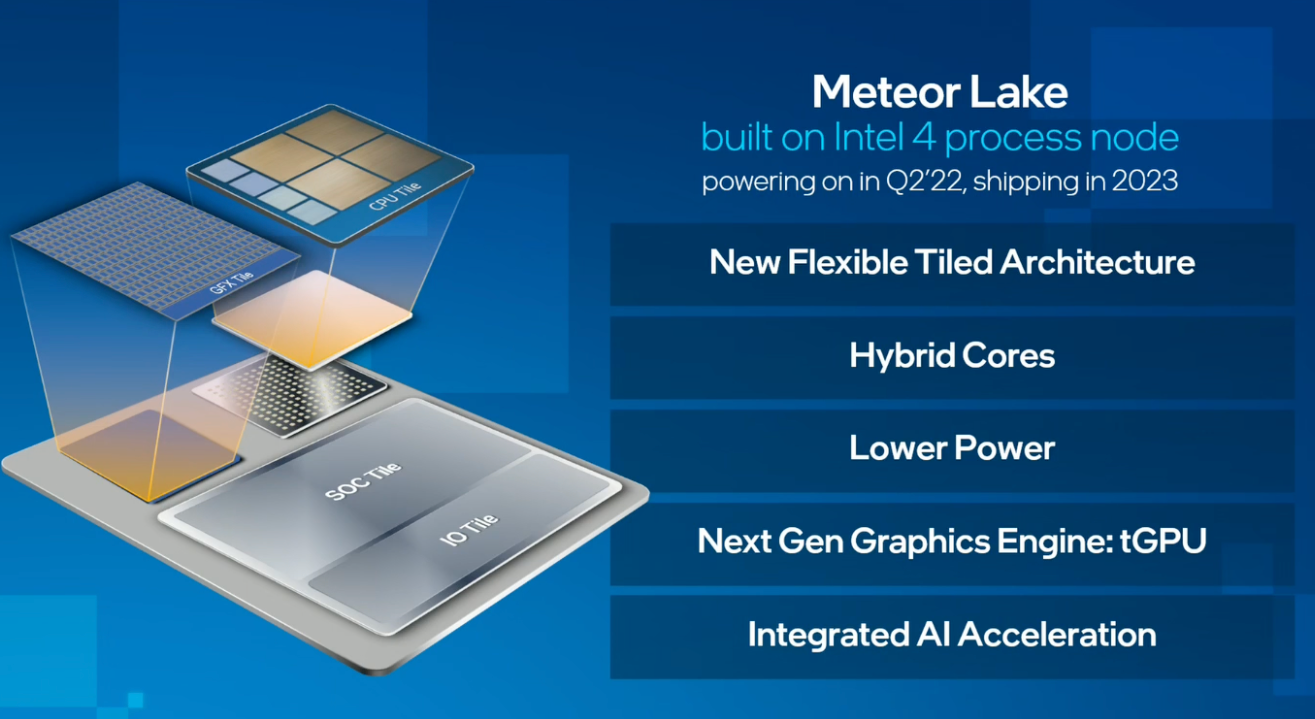
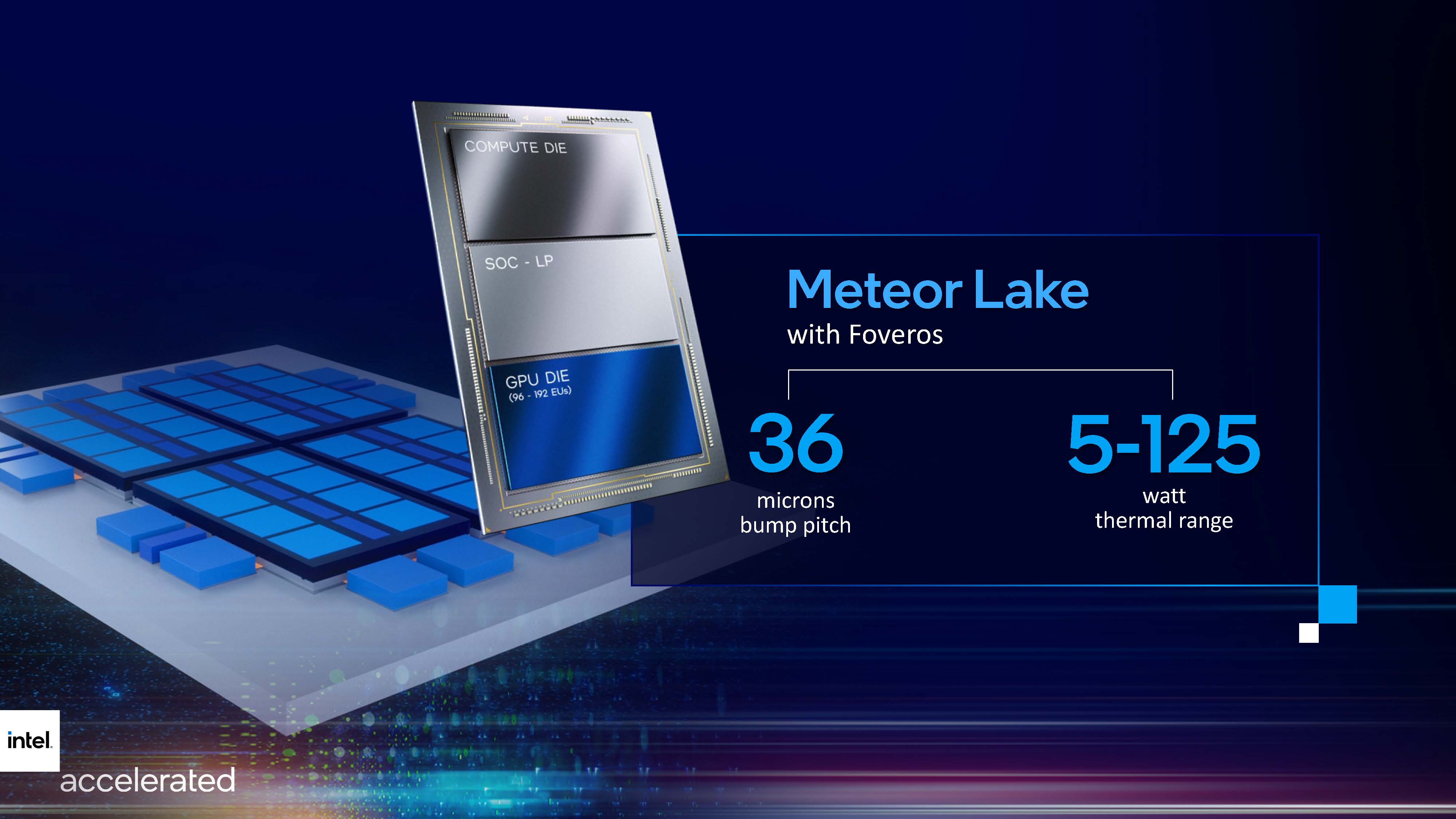
Meteor Lake first successfully booted up in Windows, Chrome, and Linux last month, and it is due to begin shipping to customers in 2023 as 14th Gen Core processors. It looks like Meteor Lake will be a mobile-first architecture, and the presentation will take place in a segment of Hot Chips devoted to mobile and edge processors. Meteor Lake chips will scale from 5W on the mobile side up to 125W for desktops.


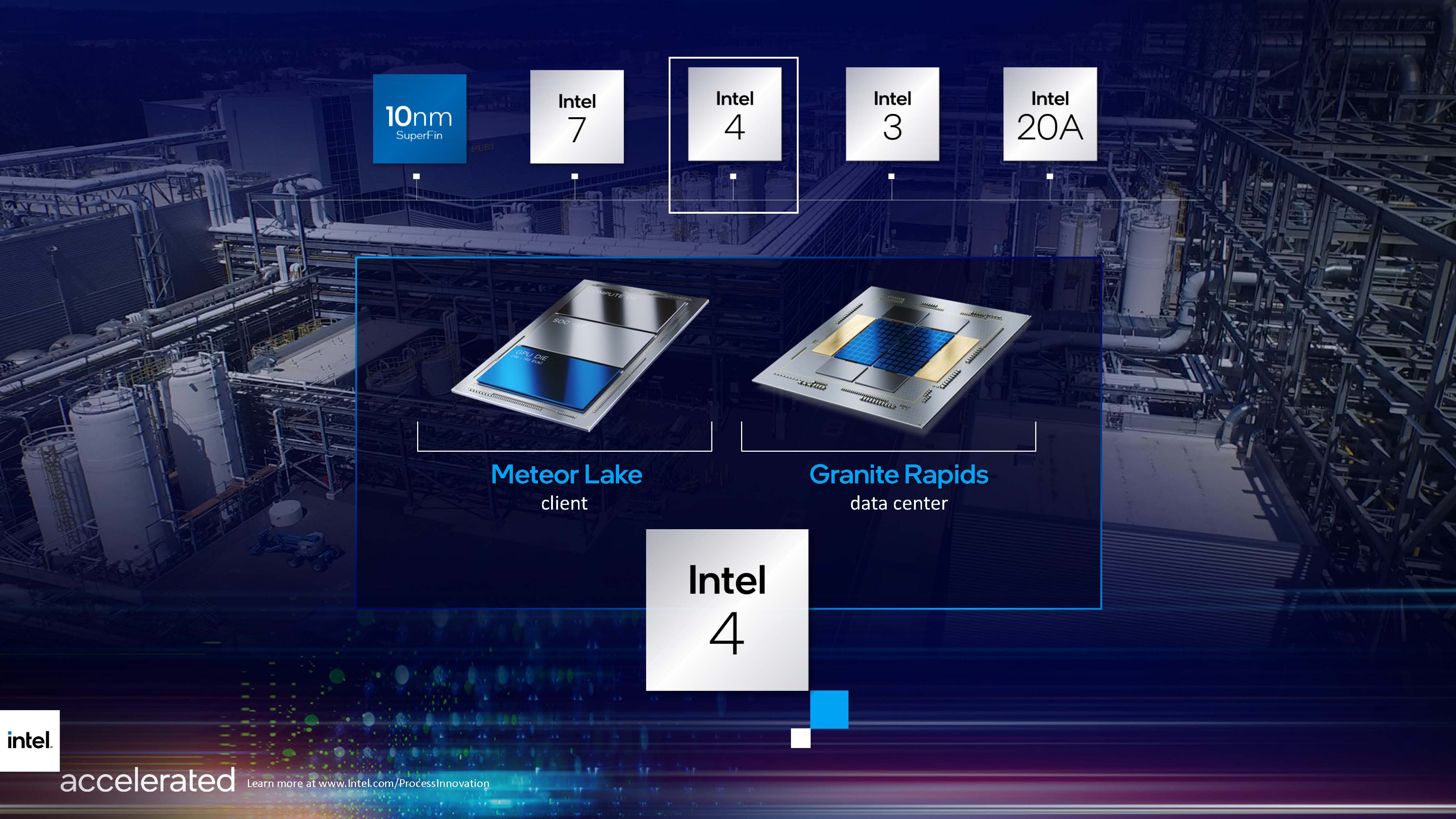
To remind readers of the importance of Meteor Lake for Intel, it will be a platform that debuts several essential technologies. Meteor Lake utilizes the Intel 4 process node. We already know it will feature a flexible tiled architecture with chiplets and hybrid cores and a next gen integrated GPU and AI acceleration (a trend set by Arm mobile processors).
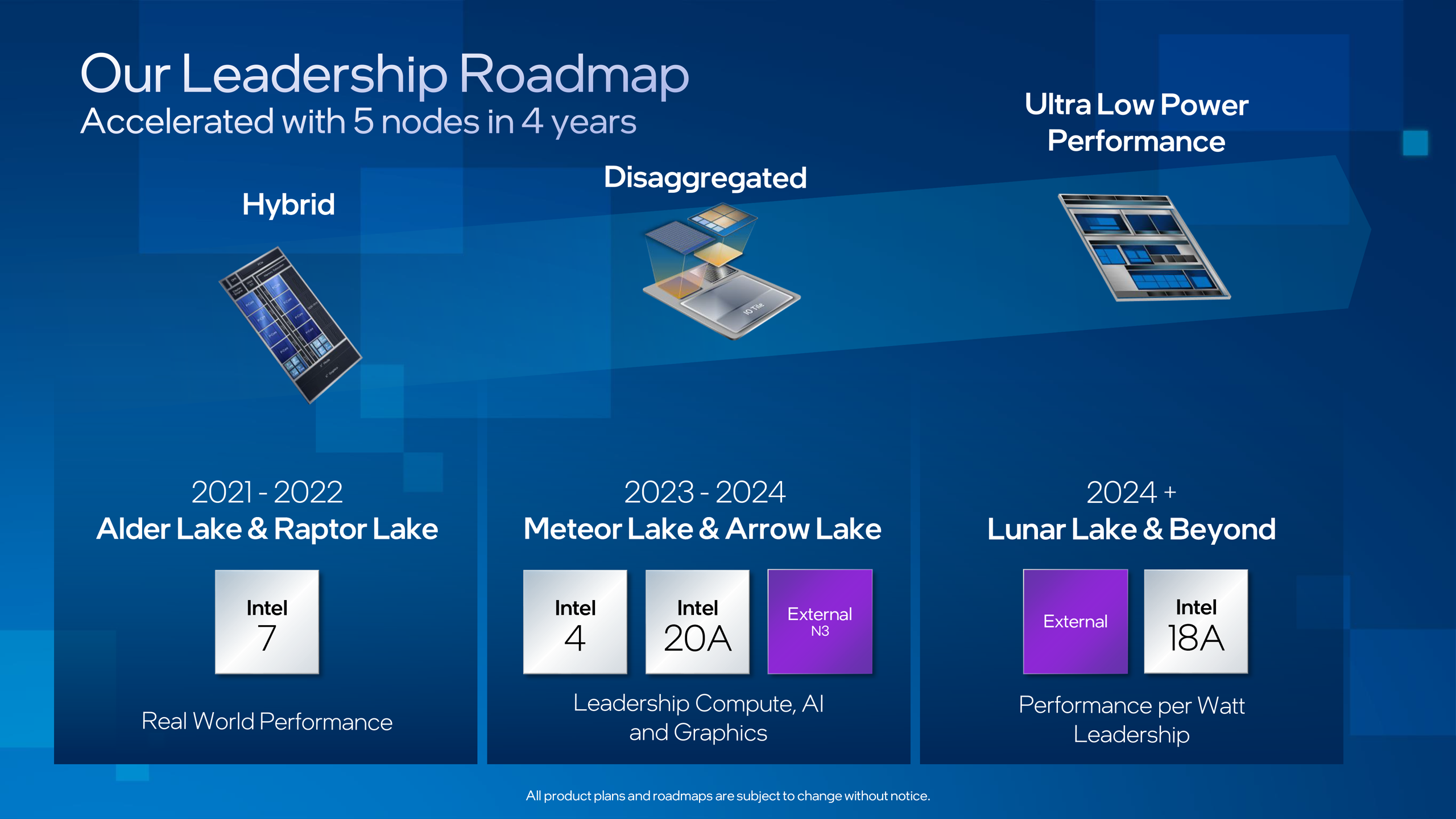
The Hot Chips 34 presentation descriptions confirm that Meteor Lake will feature a "Next Gen 3D Client Architecture Platform with Foveros," or a new generation 3D Foveros implementation, with doubled connection density compared to the previous gen. As far as we know, right now, Arrow Lake, or the 15th Gen Core processors, will carry through most of the features of Meteor Lake with a die shrink to Intel 18A. Meteor Lake and Arrow Lake might share a common platform like we have seen confirmed that Alder Lake and Raptor Lake do.
AMD, Nvidia, and Tesla
AMD will also have multiple presentations at Hot Chips. It will discuss its latest Instinct GPU accelerators for HPC on Monday. On Tuesday, it has a presentation about an SoC targeting networking hardware. Lastly, and probably the most interesting to us, will be a late Tuesday presentation about AMD Ryzen 6000 series processors (mobile). We saw this Ryzen APU family first unwrapped at CES, and they have only recently started to feature in laptop designs that are shipping. Since this presentation is part of the mobile segment, it could be that there are some more ULV models on the way. The current H-series are 35 to 45W+, and the U-series are 15-28W. Could we see some sub-15W APUs between now and the end of August?
If we had to pick a highlight from Nvidia's upcoming Hot Chips presentations, we would probably jump with both feet onto the Nvidia Grace CPU talk. We reported the 144-core Nvidia Grace CPU in quite some depth last month. However, Nvidia has promised more architectural insight later, and the Hot Chips 34 presentation looks like the right place at the right time.
Get Tom's Hardware's best news and in-depth reviews, straight to your inbox.
The Tesla Dojo features two separate presentations at Hot Chips 34. Tesla decided to split the presentations regarding this exascale computer into an architectural segment, and a super compute scaling ML training segment, led by respective experts from the company. In our most recent report on the Tesla Dojo, we talked about this 7nm and 50 billion transistor chip's custom ASIC-for-AI design and performance potential. We are looking forward to an official update on the hardware, how it will be implemented, and more.

Mark Tyson is a news editor at Tom's Hardware. He enjoys covering the full breadth of PC tech; from business and semiconductor design to products approaching the edge of reason.
-
thisisaname Intel if they can not produce the chips they can talk about how good they will be once they get around to making them :rolleyes::sneaky:Reply -
JayNor So, what would be considered 3D Foveros on that design? Are there L2 SRAM tiles in the substrate?Reply -
jkflipflop98 ReplyJayNor said:So, what would be considered 3D Foveros on that design? Are there L2 SRAM tiles in the substrate?
The base chunk that all the chiplets are plugging into is the Foveros. To oversimplify things, Foveros is a super-fancy breadboard with brains. You can plug a bunch of chips into it and they all start communicating at ultra high speeds. So you can have your logical cores built at TSMC, your GPU built inside of Intel's leading edge fabs, and a I/O chip built on an older generation process in another fab - plug them all into foveros and they'll work together as if they're a single chip.
They don't really point it out in the pictures, strangely. -
JayNor Replyjkflipflop98 said:To oversimplify things, Foveros is a super-fancy breadboard with brains.
They don't really point it out in the pictures, strangely.
thanks ... so, on Ponte Vecchio they label it as their communication fabric. -
jkflipflop98 That's a good way to put it. It's how individual "chiplets" can all talk to one another as if they're the same silicon.Reply -
cyrusfox Reply
Yep it says Foveros right next to communication fabric on this picture of Ponte Vecchio, but Ponte Vecchio also has EMIB and all that HBM making it a massive chip. Nothing like the compact pictures of Meteor lake being shown, interested to hear about the details from hot chips and future packaging plans. How do they compare to what Apple has already achieved with the M1Ultra?JayNor said:thanks ... so, on Ponte Vecchio they label it as their communication fabric. -
JayNor I ran across a techpowerup article, "Intel Details Ponte Vecchio Accelerator: 63 Tiles, 600 Watt TDP, and Lots of Bandwidth", that has the best description I've seen of the Ponte Vecchio base tile ... 17 layers, with memory controller, FIVR, power management, pcie5 16 lanes, CXL ... so they did manage to move a few items onto it.Reply -
SiliconFly Reply
Their 12th Gen Alder Lake was on schedule. The upcoming 13th Gen Raptor Lake is on schedule. Their future 14th Gen Meteor Lake is set to be released 12 months after Raptor Lake. Again on schedule.thisisaname said:Intel if they can not produce the chips they can talk about how good they will be once they get around to making them :rolleyes::sneaky:
What are you talking about? Still living in the past and believing all FUD spread by cheap AMD marketing? :rolleyes: Enter 2022! -
thisisaname Reply
I wrote that comment 4 months ago is 13th generation out now are we still hearing how good it is going to be?SiliconFly said:Their 12th Gen Alder Lake was on schedule. The upcoming 13th Gen Raptor Lake is on schedule. Their future 14th Gen Meteor Lake is set to be released 12 months after Raptor Lake. Again on schedule.
What are you talking about? Still living in the past and believing all FUD spread by cheap AMD marketing? :rolleyes: Enter 2022!
Enter the 3 quarter :geek: